

Consulte las especificaciones para obtener detalles del producto.
Encyclopedia Entry: 74V1G77STR
Product Overview
Category
The 74V1G77STR belongs to the category of integrated circuits (ICs), specifically digital logic gates.
Use
This product is commonly used in electronic devices and systems for logical operations, such as signal processing, data manipulation, and control functions.
Characteristics
- The 74V1G77STR is a single positive-edge triggered D-type flip-flop.
- It operates at a voltage range of 2.0V to 5.5V, making it compatible with various power supply levels.
- This IC has a high-speed operation capability, enabling efficient data transfer and processing.
- It offers low power consumption, making it suitable for battery-powered applications.
- The 74V1G77STR is designed to be resistant to noise and interference, ensuring reliable performance.
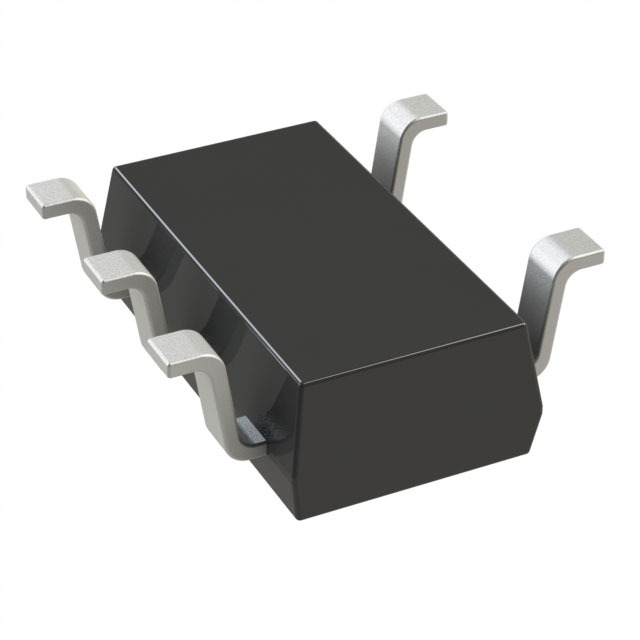
Package and Quantity
This product is available in a small-outline transistor (SOT) package, which provides compactness and ease of integration into circuit boards. It is typically supplied in tape and reel packaging, with a quantity of 3000 units per reel.
Specifications
- Supply Voltage Range: 2.0V to 5.5V
- High-Level Input Voltage: 2.0V to VCC
- Low-Level Input Voltage: GND to 0.8V
- Operating Temperature Range: -40°C to +85°C
- Output Drive Capability: ±24mA
- Propagation Delay Time: 3.5ns (typical)
Pin Configuration
The 74V1G77STR has a total of 6 pins, each serving a specific function: 1. D (Data) Input 2. CP (Clock Pulse) Input 3. Q (Output) 4. /Q (Complementary Output) 5. GND (Ground) 6. VCC (Power Supply)
Functional Features
- Positive-edge Triggered: The flip-flop captures and stores the input data on the rising edge of the clock pulse.
- Data Retention: The stored data remains stable until a new input is received.
- Complementary Outputs: The Q and /Q outputs provide inverted versions of each other, allowing for versatile signal routing.
Advantages
- Compact Size: The small-outline transistor package enables space-efficient circuit designs.
- Wide Voltage Range: The 74V1G77STR can operate within a broad voltage range, enhancing compatibility with various systems.
- Low Power Consumption: This IC minimizes energy usage, making it suitable for battery-powered devices.
- High-Speed Operation: The fast propagation delay time ensures efficient data processing.
Disadvantages
- Limited Functionality: As a single flip-flop, the 74V1G77STR may not be suitable for complex sequential logic applications that require multiple flip-flops.
Working Principles
The 74V1G77STR operates based on the principles of digital logic. It utilizes positive-edge triggering to capture and store the input data. The clock pulse synchronizes the transfer of data from the D input to the Q output. The stored data remains unchanged until a new input is received, ensuring stability during subsequent operations.
Application Field Plans
The 74V1G77STR finds application in various electronic systems, including: - Microcontrollers and microprocessors - Communication devices - Consumer electronics - Industrial automation - Automotive electronics
Alternative Models
For similar functionality, alternative models to the 74V1G77STR include: - SN74LVC1G77DBVR by Texas Instruments - MC74VHC1G77DTT1G by ON Semiconductor - CD74HCT77E by Texas Instruments
In conclusion, the 74V1G77STR is a single positive-edge triggered D-type flip-flop integrated circuit. It offers compactness, low power consumption, and high-speed operation. While it may have limited functionality for complex applications, it finds use in various electronic systems across different industries.
Word Count: 446
Enumere 10 preguntas y respuestas comunes relacionadas con la aplicación de 74V1G77STR en soluciones técnicas
Sure! Here are 10 common questions and answers related to the application of 74V1G77STR in technical solutions:
Q1: What is the 74V1G77STR? A1: The 74V1G77STR is a single positive-edge triggered D-type flip-flop with clear.
Q2: What is the purpose of the 74V1G77STR? A2: The purpose of the 74V1G77STR is to store and synchronize digital data in electronic circuits.
Q3: What voltage levels does the 74V1G77STR support? A3: The 74V1G77STR supports voltage levels ranging from 1.65V to 5.5V.
Q4: How many inputs and outputs does the 74V1G77STR have? A4: The 74V1G77STR has one data input (D), one clock input (CLK), one clear input (CLR), and one output (Q).
Q5: What is the maximum clock frequency supported by the 74V1G77STR? A5: The 74V1G77STR can operate at a maximum clock frequency of 200MHz.
Q6: Can the 74V1G77STR be used in both synchronous and asynchronous applications? A6: Yes, the 74V1G77STR can be used in both synchronous and asynchronous applications.
Q7: What is the power supply range for the 74V1G77STR? A7: The 74V1G77STR operates within a power supply range of 1.65V to 5.5V.
Q8: Does the 74V1G77STR have any special features? A8: Yes, the 74V1G77STR has a clear input (CLR) that allows the flip-flop to be reset to a known state.
Q9: Can the 74V1G77STR be cascaded with other flip-flops? A9: Yes, the 74V1G77STR can be cascaded with other flip-flops to create larger storage registers or shift registers.
Q10: What are some common applications of the 74V1G77STR? A10: The 74V1G77STR is commonly used in digital systems for data synchronization, frequency division, and general-purpose storage applications.
Please note that these questions and answers are based on general information about the 74V1G77STR. For specific technical details, it is recommended to refer to the datasheet provided by the manufacturer.