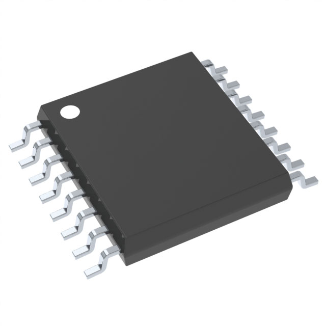
Consulte las especificaciones para obtener detalles del producto.

Encyclopedia Entry: 74AC11138PW
Basic Information Overview
- Category: Integrated Circuit (IC)
- Use: Decoder/Demultiplexer
- Characteristics:
- High-speed operation
- Low power consumption
- Wide operating voltage range
- Multiple output configurations
- Package: 16-pin TSSOP (Thin Shrink Small Outline Package)
- Essence: The 74AC11138PW is a decoder/demultiplexer IC that converts binary input signals into multiple output lines.
- Packaging/Quantity: Typically sold in reels or tubes containing multiple units.
Specifications
- Supply Voltage Range: 2V to 6V
- Input Voltage Range: 0V to VCC
- Output Voltage Range: 0V to VCC
- Maximum Operating Frequency: 125 MHz
- Number of Inputs: 3
- Number of Outputs: 8
Detailed Pin Configuration
The 74AC11138PW has 16 pins, each serving a specific function. Here is the detailed pin configuration:
- A0: Binary input line 0
- A1: Binary input line 1
- A2: Binary input line 2
- GND: Ground reference
- Y0: Output line 0
- Y1: Output line 1
- Y2: Output line 2
- Y3: Output line 3
- Y4: Output line 4
- Y5: Output line 5
- Y6: Output line 6
- Y7: Output line 7
- OE: Output Enable
- VCC: Positive supply voltage
- NC: No Connection
- NC: No Connection
Functional Features
- Decoding Function: The 74AC11138PW decodes the binary input signals (A0, A1, A2) and activates the corresponding output line(s) based on the input combination.
- Demultiplexing Function: It can also be used as a demultiplexer, where a single input line is routed to one of the multiple output lines based on the input configuration.
- Output Enable Control: The OE pin allows the user to enable or disable the outputs, providing flexibility in controlling the output state.
Advantages and Disadvantages
Advantages: - High-speed operation allows for quick signal processing. - Low power consumption helps conserve energy. - Wide operating voltage range provides compatibility with various systems. - Multiple output configurations offer versatility in signal routing.
Disadvantages: - Limited number of inputs may restrict complex decoding operations. - Lack of internal pull-up or pull-down resistors may require external components for certain applications.
Working Principles
The 74AC11138PW operates based on the principles of digital logic. The binary input signals (A0, A1, A2) are decoded internally, activating the corresponding output line(s) based on the input combination. The output state can be controlled using the OE pin, enabling or disabling the outputs as required.
Detailed Application Field Plans
The 74AC11138PW finds applications in various fields, including: 1. Address Decoding: Used in microcontrollers and memory devices to decode address signals and select specific memory locations. 2. Data Routing: Employed in communication systems to route data signals to different channels based on the input configuration. 3. Multiplexing/Demultiplexing: Utilized in data transmission systems to multiplex or demultiplex signals between different devices or subsystems.
Detailed and Complete Alternative Models
Some alternative models that provide similar functionality to the 74AC11138PW include: - 74HC138: Similar decoder/demultiplexer IC with a wider supply voltage range. - CD74AC138: Another decoder/demultiplexer IC with similar characteristics but different pin configuration. - SN74LS138: A popular TTL (Transistor-Transistor Logic) decoder/demultiplexer IC.
(Note: The above list is not exhaustive and there are several other alternative models available in the market.)
In conclusion, the 74AC11138PW is a versatile decoder/demultiplexer IC that offers high-speed operation, low power consumption, and multiple output configurations. Its wide application field plans make it suitable for various digital systems requiring signal decoding or demultiplexing capabilities.
Enumere 10 preguntas y respuestas comunes relacionadas con la aplicación de 74AC11138PW en soluciones técnicas
Sure! Here are 10 common questions and answers related to the application of 74AC11138PW in technical solutions:
Q: What is the 74AC11138PW? A: The 74AC11138PW is a 3-to-8 line decoder/demultiplexer integrated circuit (IC) commonly used in digital electronics.
Q: What is the purpose of the 74AC11138PW? A: The purpose of this IC is to decode a 3-bit binary input and activate one of the eight output lines based on the input combination.
Q: What is the maximum operating voltage for the 74AC11138PW? A: The maximum operating voltage for this IC is typically 5.5 volts.
Q: How many input pins does the 74AC11138PW have? A: This IC has three input pins, labeled A0, A1, and A2, which accept the 3-bit binary input.
Q: How many output pins does the 74AC11138PW have? A: The 74AC11138PW has eight output pins, labeled Y0 to Y7, corresponding to the eight possible output combinations.
Q: Can the 74AC11138PW be used as a demultiplexer? A: Yes, the 74AC11138PW can function as a demultiplexer by using its input pins to select one of the eight output lines.
Q: What is the typical propagation delay of the 74AC11138PW? A: The typical propagation delay of this IC is around 5 nanoseconds.
Q: Is the 74AC11138PW compatible with TTL logic levels? A: Yes, the 74AC11138PW is compatible with both TTL and CMOS logic levels.
Q: Can the 74AC11138PW be cascaded to increase the number of output lines? A: Yes, multiple 74AC11138PW ICs can be cascaded together to increase the number of output lines beyond eight.
Q: What are some common applications of the 74AC11138PW? A: Some common applications include address decoding in microprocessors, data routing in multiplexers, and general-purpose digital logic design.
Please note that the answers provided here are general and may vary depending on specific datasheet specifications and application requirements.

