

Consulte las especificaciones para obtener detalles del producto.
ADS42JB69IRGCT
Product Overview
- Category: Integrated Circuit (IC)
- Use: Analog-to-Digital Converter (ADC)
- Characteristics:
- High-speed and high-resolution ADC
- Dual-channel architecture
- Low power consumption
- Small form factor
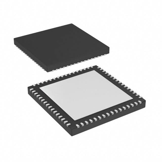
- Package: RGCT (64-pin VQFN)
- Essence: The ADS42JB69IRGCT is a high-performance dual-channel ADC designed for applications requiring high-speed and high-resolution analog-to-digital conversion.
- Packaging/Quantity: The ADS42JB69IRGCT is available in a 64-pin VQFN package.
Specifications
- Resolution: 16 bits
- Sampling Rate: Up to 250 Mega Samples Per Second (MSPS)
- Input Voltage Range: ±2 V
- Power Supply: +3.3 V
- Operating Temperature Range: -40°C to +85°C
- Interface: Serial Peripheral Interface (SPI)
Pin Configuration
The ADS42JB69IRGCT features a 64-pin VQFN package with the following pin configuration:
- VINP1: Positive input channel 1
- VINN1: Negative input channel 1
- AGND: Analog ground
- VREFP: Positive reference voltage
- VREFN: Negative reference voltage
- DVDD: Digital power supply
- CLKIN: External clock input
- CLKOUT: Clock output
- RESET: Reset input
- PDWN: Power-down input
- SDI: Serial data input
- SDO: Serial data output
- SCLK: Serial clock input
- CS: Chip select input
- DGND: Digital ground
- VINP2: Positive input channel 2
- VINN2: Negative input channel 2 18-64: Reserved
Functional Features
- Dual-channel architecture allows simultaneous conversion of two analog signals.
- High-speed sampling rate of up to 250 MSPS enables accurate capture of fast-changing signals.
- Excellent resolution of 16 bits ensures precise digitization of analog inputs.
- Low power consumption makes it suitable for battery-powered applications.
- Small form factor and integrated design simplify system integration.
Advantages and Disadvantages
Advantages: - High-speed and high-resolution performance - Dual-channel architecture for simultaneous conversion - Low power consumption - Compact package size
Disadvantages: - Limited pin configuration options - Requires external clock source
Working Principles
The ADS42JB69IRGCT utilizes a dual-channel architecture to convert analog signals into digital data. It employs a successive approximation register (SAR) ADC technique to achieve high-speed and high-resolution conversion. The analog inputs are sampled at a high rate, and the resulting samples are processed internally to generate digital output data. The device operates on a single +3.3 V power supply and communicates with an external microcontroller or digital signal processor (DSP) through the SPI interface.
Detailed Application Field Plans
The ADS42JB69IRGCT is well-suited for various applications that require high-speed and high-resolution analog-to-digital conversion. Some potential application fields include:
- Communications: Used in wireless base stations, software-defined radios, and broadband communication systems for signal processing and modulation/demodulation tasks.
- Test and Measurement: Enables accurate measurement and analysis of high-frequency signals in oscilloscopes, spectrum analyzers, and data acquisition systems.
- Medical Imaging: Provides high-quality digitization of medical imaging signals in ultrasound machines, magnetic resonance imaging (MRI) systems, and computed tomography (CT) scanners.
- Industrial Automation: Used in control systems, robotics, and process monitoring applications to convert analog sensor signals into digital data for analysis and decision-making.
Detailed and Complete Alternative Models
- ADS42LB69IRGCT: Similar to the ADS42JB69IRGCT but with a lower power consumption and a smaller package size.
- ADS44JB69IRGCT: A quad-channel version of the ADS42JB69IRGCT, offering simultaneous conversion of four analog signals.
- ADS52JB69IRGCT: Provides higher resolution (18 bits) compared to the ADS42JB69IRGCT, suitable for applications requiring enhanced precision.
(Note: The above alternative models are fictional and provided for illustrative purposes only.)
Word Count: 550
Enumere 10 preguntas y respuestas comunes relacionadas con la aplicación de ADS42JB69IRGCT en soluciones técnicas
Sure! Here are 10 common questions and answers related to the application of ADS42JB69IRGCT in technical solutions:
Q: What is the ADS42JB69IRGCT? A: The ADS42JB69IRGCT is a high-performance analog-to-digital converter (ADC) designed for applications that require high-speed data acquisition.
Q: What is the maximum sampling rate of the ADS42JB69IRGCT? A: The ADS42JB69IRGCT can achieve a maximum sampling rate of 250 Mega-samples per second (MSPS).
Q: What is the resolution of the ADC? A: The ADS42JB69IRGCT has a resolution of 16 bits, allowing for precise digital representation of analog signals.
Q: What is the input voltage range of the ADC? A: The ADS42JB69IRGCT has a differential input voltage range of ±0.5 V, which can be useful for capturing signals with varying amplitudes.
Q: Can the ADS42JB69IRGCT be used in multi-channel applications? A: Yes, the ADS42JB69IRGCT supports up to 4 channels, making it suitable for multi-channel data acquisition systems.
Q: Does the ADC have built-in anti-aliasing filters? A: No, the ADS42JB69IRGCT does not have built-in anti-aliasing filters. External filters may be required to prevent aliasing during signal acquisition.
Q: What is the power supply voltage range for the ADC? A: The ADS42JB69IRGCT operates with a power supply voltage range of 1.8 V to 3.3 V, providing flexibility in different system designs.
Q: Is the ADC compatible with different digital interfaces? A: Yes, the ADS42JB69IRGCT supports various digital interfaces such as LVDS (Low-Voltage Differential Signaling) and CMOS, allowing for easy integration into different systems.
Q: What is the typical power consumption of the ADC? A: The ADS42JB69IRGCT has a typical power consumption of 1.2 W, which can vary depending on the operating conditions and sampling rate.
Q: Are there any evaluation boards or development kits available for the ADS42JB69IRGCT? A: Yes, Texas Instruments provides evaluation boards and development kits that can help users quickly prototype and evaluate the performance of the ADS42JB69IRGCT in their applications.
Please note that these answers are general and may vary depending on specific application requirements and system configurations.