

Consulte las especificaciones para obtener detalles del producto.
CD40107BPW
Product Overview
Category
CD40107BPW belongs to the category of integrated circuits (ICs).
Use
This IC is commonly used in electronic circuits for various applications.
Characteristics
- CD40107BPW is a dual JK flip-flop with clear.
- It operates at a wide voltage range, typically between 3V and 18V.
- The IC has a high noise immunity and can withstand significant voltage fluctuations.
- It offers a low power consumption, making it suitable for battery-powered devices.
Package
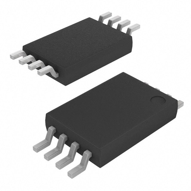
CD40107BPW is available in a 16-pin TSSOP (Thin Shrink Small Outline Package) package.
Essence
The essence of CD40107BPW lies in its ability to store and manipulate binary information using JK flip-flops.
Packaging/Quantity
The IC is typically sold in reels or tubes containing multiple units. The exact quantity may vary depending on the supplier.
Specifications
- Supply Voltage: 3V - 18V
- Operating Temperature Range: -55°C to +125°C
- Logic Family: CMOS
- Number of Pins: 16
- Flip-Flop Type: Dual JK with Clear
Detailed Pin Configuration
- CLR (Clear Input)
- CLK (Clock Input)
- J1 (J Input for Flip-Flop 1)
- K1 (K Input for Flip-Flop 1)
- Q1 (Output of Flip-Flop 1)
- Q̅1 (Complementary Output of Flip-Flop 1)
- GND (Ground)
- Q̅2 (Complementary Output of Flip-Flop 2)
- Q2 (Output of Flip-Flop 2)
- K2 (K Input for Flip-Flop 2)
- J2 (J Input for Flip-Flop 2)
- VDD (Supply Voltage) 13-16. NC (No Connection)
Functional Features
- CD40107BPW consists of two independent JK flip-flops with clear functionality.
- The flip-flops can be clocked simultaneously or asynchronously.
- The clear input allows resetting the flip-flops to a known state.
- Each flip-flop has J and K inputs, which control the output based on the clock signal.
Advantages and Disadvantages
Advantages
- Wide operating voltage range allows compatibility with various systems.
- Low power consumption makes it suitable for battery-powered devices.
- High noise immunity ensures reliable operation even in noisy environments.
Disadvantages
- Limited number of flip-flops per IC compared to larger integrated circuits.
- May require additional external components for certain applications.
Working Principles
CD40107BPW operates based on the principles of JK flip-flops. The J and K inputs control the output state based on the clock signal. The clear input resets the flip-flops to a known state when activated. The IC operates within the specified voltage range, providing reliable storage and manipulation of binary information.
Detailed Application Field Plans
CD40107BPW finds applications in various electronic circuits, including but not limited to: - Counters and frequency dividers - Data storage and retrieval systems - Sequential logic circuits - Timing and synchronization circuits
Detailed and Complete Alternative Models
Some alternative models that serve similar functions to CD40107BPW include: - SN74LS107AN - MC140107B - HEF40107BT
These alternatives offer comparable features and can be used as substitutes depending on the specific requirements of the application.
Word count: 436 words
Enumere 10 preguntas y respuestas comunes relacionadas con la aplicación de CD40107BPW en soluciones técnicas
Sure! Here are 10 common questions and answers related to the application of CD40107BPW in technical solutions:
Q: What is CD40107BPW? A: CD40107BPW is a CMOS dual 2-input NAND buffer/Driver IC, commonly used in digital logic circuits.
Q: What is the operating voltage range for CD40107BPW? A: The operating voltage range for CD40107BPW is typically between 3V and 18V.
Q: Can CD40107BPW be used as a level shifter? A: Yes, CD40107BPW can be used as a level shifter to convert signals from one voltage level to another.
Q: How many inputs does CD40107BPW have? A: CD40107BPW has two inputs per gate, making it a dual 2-input NAND buffer/Driver.
Q: What is the maximum output current of CD40107BPW? A: The maximum output current of CD40107BPW is typically around 6mA.
Q: Can CD40107BPW be used in high-frequency applications? A: CD40107BPW is not specifically designed for high-frequency applications, but it can be used in moderate-speed digital circuits.
Q: Is CD40107BPW suitable for driving capacitive loads? A: CD40107BPW can drive small capacitive loads, but for larger capacitive loads, an external buffer or driver may be required.
Q: Can CD40107BPW be used in both TTL and CMOS logic systems? A: Yes, CD40107BPW is compatible with both TTL and CMOS logic systems.
Q: What is the typical propagation delay of CD40107BPW? A: The typical propagation delay of CD40107BPW is around 20-30 nanoseconds.
Q: Can CD40107BPW be used in battery-powered applications? A: Yes, CD40107BPW can be used in battery-powered applications as it operates within a wide voltage range and has low power consumption.
Please note that these answers are general and may vary depending on specific application requirements and datasheet specifications.