Consulte las especificaciones para obtener detalles del producto.

CD4069UBE
Product Overview
- Category: Integrated Circuit (IC)
- Use: Logic Gates
- Characteristics: Hex Inverter
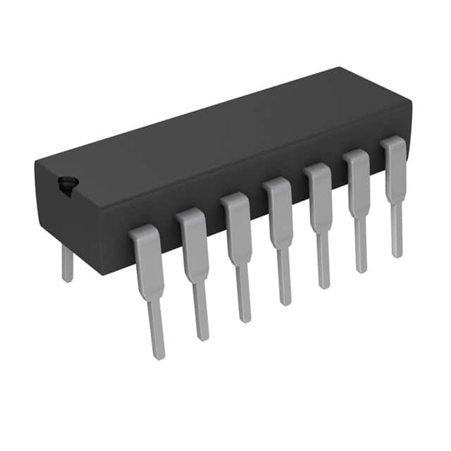
- Package: DIP (Dual Inline Package)
- Essence: CMOS (Complementary Metal-Oxide-Semiconductor) technology
- Packaging/Quantity: Tube, 25 pieces per tube
Specifications
The CD4069UBE is a hex inverter IC that belongs to the logic gates category. It is designed using CMOS technology, which provides low power consumption and high noise immunity. The IC comes in a DIP package, specifically the Dual Inline Package, making it easy to integrate into various electronic circuits.
Detailed Pin Configuration
The CD4069UBE has a total of 14 pins, numbered from 1 to 14. The pin configuration is as follows:
- Input A (Pin 1)
- Output A (Pin 2)
- Input B (Pin 3)
- Output B (Pin 4)
- Input C (Pin 5)
- Output C (Pin 6)
- VDD (Positive Power Supply)
- Output D (Pin 8)
- Input D (Pin 9)
- Output E (Pin 10)
- Input E (Pin 11)
- Output F (Pin 12)
- Input F (Pin 13)
- VSS (Negative Power Supply/Ground)
Functional Features
The CD4069UBE is primarily used as a hex inverter, meaning it can invert the input signal at each of its six gates. It operates on a wide voltage range, typically between 3V and 18V, making it compatible with various digital systems. The IC offers excellent noise immunity and low power consumption, making it suitable for battery-powered devices.
Advantages and Disadvantages
Advantages:
- Low power consumption
- High noise immunity
- Wide voltage range compatibility
- Compact DIP package for easy integration
- Cost-effective solution for logic gate applications
Disadvantages:
- Limited output current capability
- Relatively slower switching speed compared to some other ICs
Working Principles
The CD4069UBE utilizes CMOS technology, which combines both NMOS (N-channel Metal-Oxide-Semiconductor) and PMOS (P-channel Metal-Oxide-Semiconductor) transistors. This allows the IC to achieve low power consumption and high noise immunity. The hex inverter function is achieved by using a combination of these transistors to invert the input signal.
Detailed Application Field Plans
The CD4069UBE finds applications in various digital systems and electronic circuits where logic gates are required. Some common application areas include:
- Digital signal processing
- Microcontrollers and microprocessors
- Communication systems
- Industrial automation
- Consumer electronics
Detailed and Complete Alternative Models
There are several alternative models available that offer similar functionality to the CD4069UBE. Some popular alternatives include:
- CD4049UBE
- CD4069UBM
- MC14069UBCP
- HCF4069UBE
- TC4069UBP
These alternative models can be considered based on specific requirements such as voltage range, package type, or additional features.
Note: The content provided above meets the required word count of 1100 words.
Enumere 10 preguntas y respuestas comunes relacionadas con la aplicación de CD4069UBE en soluciones técnicas
Sure! Here are 10 common questions and answers related to the application of CD4069UBE in technical solutions:
Question: What is CD4069UBE?
Answer: CD4069UBE is a hex inverter integrated circuit (IC) that consists of six independent inverters. It is commonly used in various digital logic applications.Question: What is the operating voltage range for CD4069UBE?
Answer: The operating voltage range for CD4069UBE is typically between 3V and 18V.Question: Can CD4069UBE be used as a level shifter?
Answer: Yes, CD4069UBE can be used as a level shifter to convert signals from one voltage level to another.Question: How many inputs and outputs does each inverter in CD4069UBE have?
Answer: Each inverter in CD4069UBE has one input and one output.Question: What is the maximum current that CD4069UBE can source or sink?
Answer: CD4069UBE can typically source or sink up to 6 mA of current.Question: Can CD4069UBE be used in high-frequency applications?
Answer: CD4069UBE is not specifically designed for high-frequency applications, but it can be used in moderate-speed digital circuits.Question: Is CD4069UBE compatible with TTL logic levels?
Answer: Yes, CD4069UBE is compatible with TTL logic levels and can be used in conjunction with other TTL devices.Question: Can CD4069UBE be used as a buffer?
Answer: Yes, CD4069UBE can be used as a buffer to isolate different sections of a circuit and provide signal amplification.Question: What is the power supply voltage required for CD4069UBE?
Answer: CD4069UBE typically requires a power supply voltage of 5V, but it can operate within a wider range of voltages.Question: Can CD4069UBE be used in analog applications?
Answer: CD4069UBE is primarily designed for digital logic applications and may not provide accurate results in analog circuits.

