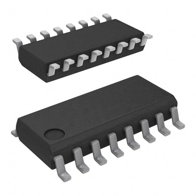
Consulte las especificaciones para obtener detalles del producto.

CD74ACT283M
Overview
- Category: Integrated Circuit (IC)
- Use: Arithmetic Logic Unit (ALU)
- Characteristics: High-speed, low-power consumption
- Package: 16-pin SOIC (Small Outline Integrated Circuit)
- Essence: Performs arithmetic and logic operations on binary numbers
- Packaging/Quantity: Available in reels of 2500 units
Specifications
- Supply Voltage: 4.5V to 5.5V
- Logic Family: ACT (Advanced CMOS Technology)
- Number of Inputs: 8
- Number of Outputs: 4
- Operating Temperature Range: -40°C to +85°C
- Propagation Delay: 6 ns (typical)
Pin Configuration
The CD74ACT283M has a 16-pin SOIC package with the following pin configuration:
- Carry Input (Cn)
- A3 Input
- A2 Input
- A1 Input
- A0 Input
- B3 Input
- B2 Input
- B1 Input
- B0 Input
- Sum Output (S3)
- Sum Output (S2)
- Sum Output (S1)
- Sum Output (S0)
- Carry Output (Cout)
- GND (Ground)
- VCC (Power Supply)
Functional Features
- Performs binary addition of two 4-bit numbers (A and B)
- Generates a 4-bit sum output (S) and a carry output (Cout)
- Supports cascading multiple ICs for larger bit-width addition
- Utilizes advanced CMOS technology for high-speed operation
- Low power consumption makes it suitable for battery-powered devices
Advantages
- High-speed operation enables efficient computation
- Low power consumption prolongs battery life in portable devices
- Compact 16-pin SOIC package saves board space
- Wide operating temperature range allows for versatile applications
Disadvantages
- Limited to 4-bit addition, not suitable for larger bit-width calculations
- Requires external circuitry for carry-in and carry-out connections in cascaded configurations
Working Principles
The CD74ACT283M is an Arithmetic Logic Unit (ALU) integrated circuit that performs binary addition of two 4-bit numbers. It utilizes advanced CMOS technology, which provides high-speed operation while consuming low power.
The ALU takes two 4-bit inputs (A and B) and generates a 4-bit sum output (S) along with a carry output (Cout). The carry input (Cn) allows cascading multiple ICs for larger bit-width addition.
During operation, the ALU adds corresponding bits of A and B, taking into account the carry input. The sum output represents the result of the addition, while the carry output indicates whether there was a carry-over from the most significant bit.
Detailed Application Field Plans
The CD74ACT283M is commonly used in various digital systems that require arithmetic operations. Some application fields include:
- Microcontrollers: Used for performing mathematical calculations in embedded systems.
- Digital Signal Processing: Enables addition operations in signal processing algorithms.
- Computer Arithmetic Units: Utilized in CPUs for executing arithmetic instructions.
- Calculator Circuits: Integrated into calculators for adding binary numbers.
- Data Encryption: Supports addition operations in cryptographic algorithms.
Detailed and Complete Alternative Models
- SN74ACT283: Similar 4-bit ALU IC from Texas Instruments.
- MC74ACT283: Equivalent 4-bit ALU IC from ON Semiconductor.
- CD74HCT283: 4-bit ALU IC with different logic family (HCT) from Texas Instruments.
These alternative models provide similar functionality and can be used as replacements for the CD74ACT283M in various applications.
Word count: 511 words
Enumere 10 preguntas y respuestas comunes relacionadas con la aplicación de CD74ACT283M en soluciones técnicas
Sure! Here are 10 common questions and answers related to the application of CD74ACT283M in technical solutions:
Q: What is CD74ACT283M? A: CD74ACT283M is a 4-bit binary full adder with fast carry. It is commonly used in digital circuits for arithmetic operations.
Q: What is the operating voltage range of CD74ACT283M? A: The operating voltage range of CD74ACT283M is typically between 4.5V and 5.5V.
Q: What is the maximum clock frequency supported by CD74ACT283M? A: CD74ACT283M can typically support clock frequencies up to 100 MHz.
Q: How many inputs and outputs does CD74ACT283M have? A: CD74ACT283M has four inputs (A, B, C0, and CI) and two outputs (S and C4).
Q: Can CD74ACT283M be cascaded to perform multi-bit addition? A: Yes, CD74ACT283M can be cascaded to perform multi-bit addition by connecting the carry output (C4) of one chip to the carry input (CI) of the next chip.
Q: What is the propagation delay of CD74ACT283M? A: The propagation delay of CD74ACT283M is typically around 7 ns.
Q: Is CD74ACT283M compatible with TTL logic levels? A: Yes, CD74ACT283M is compatible with TTL logic levels, making it suitable for interfacing with other TTL devices.
Q: Can CD74ACT283M be used in high-speed applications? A: Yes, CD74ACT283M is designed for high-speed operation, making it suitable for use in applications that require fast arithmetic calculations.
Q: Does CD74ACT283M have any built-in error detection or correction features? A: No, CD74ACT283M does not have any built-in error detection or correction features. It performs basic binary addition without error checking.
Q: What is the package type of CD74ACT283M? A: CD74ACT283M is available in various package types, such as SOIC (Small Outline Integrated Circuit) and PDIP (Plastic Dual In-line Package).
Please note that the answers provided here are general and may vary depending on the specific datasheet and manufacturer's specifications for CD74ACT283M.

