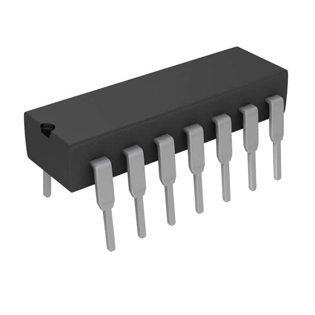
Consulte las especificaciones para obtener detalles del producto.

CD74HC126EG4
Product Overview
- Category: Integrated Circuit
- Use: Logic Gate Buffer/Driver
- Characteristics: High-Speed, CMOS Technology
- Package: SOIC (Small Outline Integrated Circuit)
- Essence: Quad 3-State Non-Inverting Buffer
- Packaging/Quantity: Tape and Reel, 2500 pieces per reel
Specifications
- Supply Voltage: 2V to 6V
- Input Voltage: 0V to Vcc
- Output Voltage: 0V to Vcc
- Operating Temperature: -40°C to +85°C
- Propagation Delay: 9ns (typical)
- Output Current: ±6mA
- Input Capacitance: 3.5pF (typical)
Pin Configuration
The CD74HC126EG4 has a total of 14 pins arranged in a dual in-line package (DIP). The pin configuration is as follows:
- 1A - Input 1 for Buffer A
- 1Y - Output for Buffer A
- GND - Ground
- 2Y - Output for Buffer B
- 2A - Input 2 for Buffer B
- 3A - Input 3 for Buffer C
- 3Y - Output for Buffer C
- Vcc - Positive Power Supply
- 4Y - Output for Buffer D
- 4A - Input 4 for Buffer D
- OE - Output Enable
- NC - No Connection
- NC - No Connection
- GND - Ground
Functional Features
- Quad 3-state non-inverting buffer
- High-speed operation
- Compatible with CMOS logic levels
- Output can drive up to ±6mA
- Output can be disabled using the OE pin
Advantages and Disadvantages
Advantages
- High-speed operation allows for efficient data transfer
- CMOS technology provides low power consumption
- 3-state output allows for bus sharing and multiple device connections
- Wide operating voltage range (2V to 6V) offers flexibility in various applications
Disadvantages
- Limited output current may not be suitable for high-power applications
- Propagation delay of 9ns may cause timing issues in certain scenarios
- Not compatible with TTL logic levels
Working Principles
The CD74HC126EG4 is a quad 3-state non-inverting buffer that operates using CMOS technology. It takes input signals from four different sources and provides buffered outputs. The output can be enabled or disabled using the OE pin. When the OE pin is high, the outputs are active, and when it is low, the outputs are in a high-impedance state.
Detailed Application Field Plans
The CD74HC126EG4 is commonly used in various digital systems and electronic devices. Some of its application fields include:
- Data communication systems
- Microcontrollers and microprocessors
- Memory interfaces
- Industrial automation
- Automotive electronics
- Consumer electronics
Detailed and Complete Alternative Models
- SN74HC126N: DIP package, similar specifications
- MC74HC126AN: DIP package, similar specifications
- 74HCT126: DIP package, compatible with TTL logic levels
These alternative models offer similar functionality and can be used as replacements for the CD74HC126EG4 depending on specific requirements.
In conclusion, the CD74HC126EG4 is a versatile integrated circuit that serves as a quad 3-state non-inverting buffer. Its high-speed operation, compatibility with CMOS logic levels, and wide operating voltage range make it suitable for various digital systems and electronic devices. However, its limited output current and propagation delay should be considered when selecting this IC for specific applications.
Enumere 10 preguntas y respuestas comunes relacionadas con la aplicación de CD74HC126EG4 en soluciones técnicas
Sure! Here are 10 common questions and answers related to the application of CD74HC126EG4 in technical solutions:
Question: What is CD74HC126EG4?
Answer: CD74HC126EG4 is a quad buffer/line driver with 3-state outputs, commonly used in digital logic applications.Question: What is the operating voltage range for CD74HC126EG4?
Answer: The operating voltage range for CD74HC126EG4 is typically between 2V and 6V.Question: What is the maximum output current that CD74HC126EG4 can handle?
Answer: CD74HC126EG4 can handle a maximum output current of 8mA per channel.Question: Can CD74HC126EG4 be used as a level shifter?
Answer: Yes, CD74HC126EG4 can be used as a level shifter to convert signals between different voltage levels.Question: How many channels does CD74HC126EG4 have?
Answer: CD74HC126EG4 has four independent channels, each with a separate input and output.Question: What is the typical propagation delay of CD74HC126EG4?
Answer: The typical propagation delay of CD74HC126EG4 is around 9ns.Question: Is CD74HC126EG4 compatible with TTL logic levels?
Answer: Yes, CD74HC126EG4 is compatible with both CMOS and TTL logic levels.Question: Can CD74HC126EG4 be used in high-speed applications?
Answer: Yes, CD74HC126EG4 is suitable for high-speed applications due to its fast switching speed.Question: Does CD74HC126EG4 have built-in protection features?
Answer: CD74HC126EG4 has built-in diode clamps to protect against static discharge and overvoltage.Question: What is the package type for CD74HC126EG4?
Answer: CD74HC126EG4 is available in a standard 14-pin SOIC (Small Outline Integrated Circuit) package.
Please note that these answers are general and may vary depending on specific datasheet specifications and application requirements.

