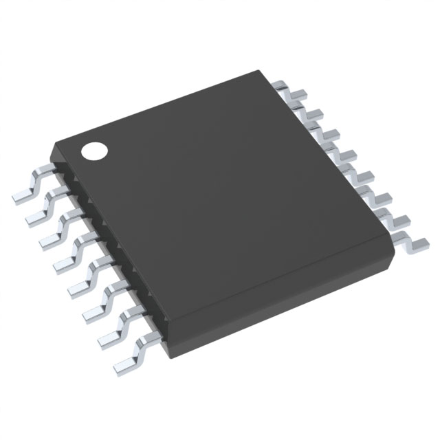
Consulte las especificaciones para obtener detalles del producto.

CDCE925PWG4
Overview
CDCE925PWG4 is a product belonging to the category of integrated circuits. It is commonly used in electronic devices for clock generation and synchronization purposes. This integrated circuit offers various characteristics that make it suitable for a wide range of applications. The package of CDCE925PWG4 consists of a small form factor, allowing for easy integration into electronic systems. Its essence lies in its ability to generate precise clock signals, which are essential for the proper functioning of digital circuits. The packaging/quantity of CDCE925PWG4 typically includes a single unit.
Specifications and Parameters
- Input Voltage Range: 2.5V to 3.6V
- Output Frequency Range: 1MHz to 200MHz
- Operating Temperature Range: -40°C to +85°C
- Supply Current: 20mA (typical)
- Package Type: TSSOP-16
Pin Configuration
The pin configuration of CDCE925PWG4 is as follows:
- VDDA
- GND
- XIN
- XOUT
- CLK0_OUT
- CLK1_OUT
- CLK2_OUT
- CLK3_OUT
- CLK4_OUT
- CLK5_OUT
- CLK6_OUT
- CLK7_OUT
- SDA
- SCL
- OE
- VDDD
Functional Characteristics
CDCE925PWG4 offers the following functional characteristics:
- Clock multiplication and division
- Programmable output frequencies
- Low jitter performance
- I2C interface for configuration
- Power-down mode for reduced power consumption
Advantages and Disadvantages
Advantages: - Precise clock signal generation - Flexible frequency configuration - Low jitter performance - Compact package size
Disadvantages: - Requires external crystal oscillator - Limited output frequency range
Applicable Range of Products
CDCE925PWG4 is widely applicable in various electronic devices that require accurate clock generation and synchronization. It is commonly used in telecommunications equipment, networking devices, consumer electronics, and industrial automation systems.
Working Principles
The CDCE925PWG4 operates by taking an input clock signal and generating multiple output clock signals with different frequencies. It achieves this through a combination of frequency multiplication and division techniques. The integrated circuit also allows for the precise configuration of output frequencies using the I2C interface.
Detailed Application Field Plans
CDCE925PWG4 can be utilized in a variety of applications, including:
- Telecommunications: Providing synchronized clock signals for data transmission and reception.
- Networking: Clock synchronization in routers, switches, and network interface cards.
- Consumer Electronics: Clock generation for audio/video processing, digital displays, and multimedia devices.
- Industrial Automation: Timing and synchronization in control systems, PLCs, and motor drives.
- Test and Measurement: Precise timing for data acquisition, signal analysis, and test equipment.
Detailed Alternative Models
Some alternative models to CDCE925PWG4 include:
- CDCE913PWG4
- CDCE937PWG4
- CDCE949PWG4
- CDCE961PWG4
- CDCE973PWG4
5 Common Technical Questions and Answers
Q: Can CDCE925PWG4 operate with a single power supply? A: Yes, it can operate with a single power supply within the specified voltage range.
Q: What is the maximum output frequency that CDCE925PWG4 can generate? A: CDCE925PWG4 can generate output frequencies up to 200MHz.
Q: Is CDCE925PWG4 compatible with both 3.3V and 5V logic levels? A: Yes, it is compatible with both 3.3V and 5V logic levels.
Q: Can CDCE925PWG4 be used in battery-powered devices? A: Yes, CDCE925PWG4 has a low supply current and can be used in battery-powered devices.
Q: Does CDCE925PWG4 support frequency synchronization from an external source? A: No, CDCE925PWG4 does not support frequency synchronization from an external source.
This concludes the encyclopedia entry for CDCE925PWG4.
Word count: 511

