

Consulte las especificaciones para obtener detalles del producto.
LMX2335USLBX
Overview
Category
LMX2335USLBX belongs to the category of integrated circuits (ICs).
Use
This product is commonly used in electronic devices for frequency synthesis and phase-locked loop (PLL) applications.
Characteristics
LMX2335USLBX exhibits the following characteristics: - High precision frequency synthesis - Low phase noise - Wide frequency range - Low power consumption
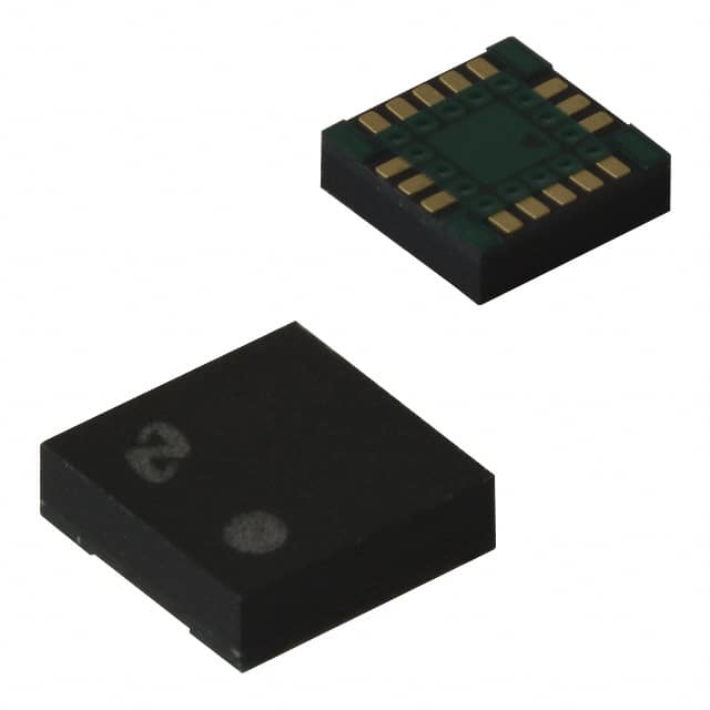
Package
LMX2335USLBX is available in a small outline integrated circuit (SOIC) package.
Essence
The essence of LMX2335USLBX lies in its ability to generate stable and accurate frequencies for various applications.
Packaging/Quantity
This product is typically packaged in reels or tubes, with a quantity of 250 units per reel/tube.
Specifications and Parameters
The specifications and parameters of LMX2335USLBX include: - Frequency range: 10 MHz to 6 GHz - Output power: -4 dBm to +7 dBm - Supply voltage: 2.7 V to 3.6 V - Operating temperature range: -40°C to +85°C
Pin Configuration
The pin configuration of LMX2335USLBX is as follows:
| Pin Number | Pin Name | Description | |------------|----------|-------------| | 1 | VCC | Power supply voltage input | | 2 | GND | Ground | | 3 | RFOUT | RF output | | 4 | CE | Chip enable | | 5 | CLKIN | Reference clock input | | 6 | RFIN | RF input | | 7 | DVDD | Digital power supply voltage input | | 8 | DGND | Digital ground |
Functional Characteristics
LMX2335USLBX offers the following functional characteristics: - Frequency synthesis with fractional-N PLL - Programmable frequency divider - Phase detector for phase-locked loop operation - Integrated voltage-controlled oscillator (VCO) - Serial interface for control and configuration
Advantages and Disadvantages
Advantages
- High precision frequency synthesis
- Low phase noise
- Wide frequency range coverage
- Low power consumption
Disadvantages
- Limited output power range
- Requires external components for complete functionality
Applicable Range of Products
LMX2335USLBX is suitable for use in various electronic devices that require stable and accurate frequency generation, such as: - Wireless communication systems - Satellite communication equipment - Test and measurement instruments - Radar systems - Radio transceivers
Working Principles
The working principle of LMX2335USLBX involves the following steps: 1. The reference clock signal is provided through the CLKIN pin. 2. The phase detector compares the reference clock with the divided feedback signal from the VCO. 3. The phase error is processed by the charge pump and loop filter to generate a control voltage for the VCO. 4. The VCO generates an output frequency based on the control voltage. 5. The output frequency is divided by the programmable frequency divider to achieve the desired frequency.
Detailed Application Field Plans
LMX2335USLBX can be applied in the following fields:
Wireless Communication Systems
In wireless communication systems, LMX2335USLBX can be used for frequency synthesis in transmitters and receivers, ensuring accurate and stable signal transmission.
Satellite Communication Equipment
For satellite communication equipment, LMX2335USLBX enables precise frequency generation for uplink and downlink signals, enhancing overall system performance.
Test and Measurement Instruments
In test and measurement instruments, LMX2335USLBX can be utilized to generate stable and precise frequencies for signal analysis, calibration, and testing purposes.
Radar Systems
LMX2335USLBX finds application in radar systems where accurate frequency synthesis is crucial for target detection, tracking, and signal processing.
Radio Transceivers
In radio transceivers, LMX2335USLBX ensures reliable and accurate frequency generation for seamless communication between devices.
Detailed Alternative Models
Some alternative models to LMX2335USLBX include: - LMX2594 - ADF4351 - MAX2870 - HMC830 - Si5351
5 Common Technical Questions and Answers
Q: What is the maximum output power of LMX2335USLBX? A: The maximum output power is +7 dBm.
Q: What is the operating voltage range for this product? A: LMX2335USLBX operates within a voltage range of 2.7 V to 3.6 V.
Q: Can LMX2335USLBX operate at temperatures below freezing point?