

Consulte las especificaciones para obtener detalles del producto.
SN74ABT821ANSR
Product Overview
- Category: Integrated Circuit (IC)
- Use: Logic Gates
- Characteristics: High-speed, low-power, and high-performance
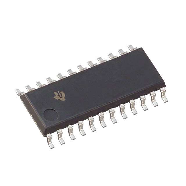
- Package: Surface Mount Technology (SMT)
- Essence: 10-bit D-type flip-flop with 3-state outputs
- Packaging/Quantity: Tape and Reel, 2,500 units per reel
Specifications
- Supply Voltage Range: 4.5V to 5.5V
- Input Voltage Range: 0V to VCC
- Output Voltage Range: 0V to VCC
- Operating Temperature Range: -40°C to +85°C
- Propagation Delay Time: 3.8ns (typical)
- Output Current: ±24mA
- Input Capacitance: 4pF (typical)
Detailed Pin Configuration
The SN74ABT821ANSR has a total of 20 pins, which are assigned as follows:
- CLK (Clock Input)
- CP (Clock Pulse Input)
- D0-D9 (Data Inputs)
- Q0-Q9 (Flip-Flop Outputs)
- G (Output Enable)
- VCC (Positive Power Supply)
- GND (Ground)
Functional Features
- High-speed operation allows for efficient data processing.
- Low-power consumption makes it suitable for battery-powered devices.
- 3-state outputs provide flexibility in connecting multiple devices.
- D-type flip-flop design ensures reliable data storage.
Advantages and Disadvantages
Advantages: - High-speed performance enables quick data processing. - Low-power consumption prolongs battery life. - 3-state outputs allow for easy integration with other devices. - Reliable data storage ensures accurate information handling.
Disadvantages: - Limited voltage range may restrict compatibility with certain systems. - SMT packaging may require specialized equipment for assembly and repair.
Working Principles
The SN74ABT821ANSR operates based on the principles of digital logic. The clock input (CLK) and clock pulse input (CP) control the timing of data storage and retrieval. When the clock signal is active, the data inputs (D0-D9) are latched into the flip-flop, and the corresponding outputs (Q0-Q9) reflect the stored data. The output enable (G) pin allows the outputs to be either enabled or disabled, providing flexibility in connecting multiple devices.
Detailed Application Field Plans
The SN74ABT821ANSR can be used in various applications, including:
- Data communication systems
- Microprocessor-based systems
- Industrial automation
- Automotive electronics
- Consumer electronics
In data communication systems, this IC can be utilized for efficient data buffering and synchronization. In microprocessor-based systems, it can serve as a reliable storage element for critical data. In industrial automation, it can facilitate precise control and timing operations. In automotive electronics, it can contribute to the functionality of safety systems. In consumer electronics, it can be employed for high-speed data processing in multimedia devices.
Detailed and Complete Alternative Models
- SN74ABT821ADWR: SOIC package, 20 pins
- SN74ABT821ADBRE4: SSOP package, 20 pins
- SN74ABT821APW: TSSOP package, 20 pins
- SN74ABT821ANSRG4: Tape and Reel packaging, 2,500 units per reel
These alternative models offer similar functionality and characteristics, providing options for different packaging requirements and pin configurations.
Word count: 430 words
Enumere 10 preguntas y respuestas comunes relacionadas con la aplicación de SN74ABT821ANSR en soluciones técnicas
Sure! Here are 10 common questions and answers related to the application of SN74ABT821ANSR in technical solutions:
Q: What is SN74ABT821ANSR? A: SN74ABT821ANSR is a specific model of integrated circuit (IC) that belongs to the ABT family of high-speed, low-power devices.
Q: What is the purpose of SN74ABT821ANSR? A: SN74ABT821ANSR is a data flip-flop IC used for storing and transferring binary data in digital systems.
Q: What is the maximum operating frequency of SN74ABT821ANSR? A: The maximum operating frequency of SN74ABT821ANSR is typically around 200 MHz.
Q: What is the voltage supply range for SN74ABT821ANSR? A: SN74ABT821ANSR operates with a voltage supply range of 4.5V to 5.5V.
Q: How many flip-flops are present in SN74ABT821ANSR? A: SN74ABT821ANSR consists of eight individual flip-flops.
Q: Can SN74ABT821ANSR be cascaded to increase the number of flip-flops? A: Yes, SN74ABT821ANSR can be cascaded to create larger registers or shift registers by connecting the output of one IC to the input of another.
Q: What is the output drive capability of SN74ABT821ANSR? A: SN74ABT821ANSR has a typical output drive capability of ±12mA.
Q: Does SN74ABT821ANSR have any built-in protection features? A: Yes, SN74ABT821ANSR has built-in protection against electrostatic discharge (ESD) and latch-up.
Q: Can SN74ABT821ANSR be used in both synchronous and asynchronous applications? A: Yes, SN74ABT821ANSR can be used in both synchronous and asynchronous applications depending on the system requirements.
Q: What are some typical applications of SN74ABT821ANSR? A: SN74ABT821ANSR is commonly used in various digital systems such as microprocessors, data storage devices, communication equipment, and control systems.
Please note that the answers provided here are general and may vary based on specific design considerations and application requirements. It is always recommended to refer to the datasheet and consult with technical experts for accurate information.