Consulte las especificaciones para obtener detalles del producto.

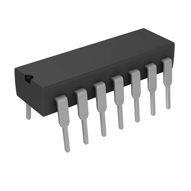
SN74AC08N
Product Overview
Category
SN74AC08N belongs to the category of integrated circuits (ICs).
Use
This IC is commonly used as a quad 2-input AND gate.
Characteristics
- High-speed operation
- Low power consumption
- Wide operating voltage range
- Schmitt-trigger inputs for noise immunity
- Compatible with TTL and CMOS logic levels
Package
SN74AC08N is available in a 14-pin DIP (Dual In-line Package) format.
Essence
The essence of SN74AC08N lies in its ability to perform logical AND operations on two input signals.
Packaging/Quantity
SN74AC08N is typically sold in reels or tubes, containing multiple units per package.
Specifications
- Supply Voltage: 2V to 6V
- Input Voltage: 0V to VCC
- Output Voltage: 0V to VCC
- Operating Temperature Range: -40°C to +85°C
- Propagation Delay Time: 3.5ns (typical)
- Maximum Quiescent Current: 4μA
Detailed Pin Configuration
SN74AC08N consists of 14 pins, each serving a specific purpose:
- Input A1
- Input B1
- Output Y1
- Ground (GND)
- Input A2
- Input B2
- Output Y2
- VCC (Positive Power Supply)
- Input A3
- Input B3
- Output Y3
- Input A4
- Input B4
- Output Y4
Functional Features
- Quad 2-input AND gate functionality
- High-speed operation allows for quick signal processing
- Low power consumption makes it suitable for battery-powered devices
- Schmitt-trigger inputs provide noise immunity, ensuring reliable operation
- Wide operating voltage range allows compatibility with various systems
Advantages and Disadvantages
Advantages
- High-speed operation enables efficient signal processing
- Low power consumption prolongs battery life in portable devices
- Wide operating voltage range ensures compatibility with different systems
- Schmitt-trigger inputs enhance noise immunity, improving reliability
Disadvantages
- Limited number of inputs (2 per gate)
- Not suitable for applications requiring more complex logic operations
Working Principles
SN74AC08N operates based on the principles of digital logic. It performs logical AND operations on two input signals, producing an output signal that is high only when both inputs are high.
Detailed Application Field Plans
SN74AC08N finds application in various fields, including:
- Digital electronics: Used in logic circuits to perform AND operations.
- Microcontrollers: Employed to interface with other components and perform logical operations.
- Communication systems: Utilized in signal processing and data transmission circuits.
- Industrial automation: Integrated into control systems for logical decision-making.
Detailed and Complete Alternative Models
Some alternative models to SN74AC08N include:
- 74HC08: Similar quad 2-input AND gate IC with CMOS technology.
- CD4081: Quad 2-input AND gate IC with higher voltage tolerance.
- SN54AC08: Equivalent to SN74AC08N but designed for military applications.
These alternative models offer similar functionality but may differ in terms of voltage range, speed, or specific application focus.
Word count: 431 words
Enumere 10 preguntas y respuestas comunes relacionadas con la aplicación de SN74AC08N en soluciones técnicas
Sure! Here are 10 common questions and answers related to the application of SN74AC08N:
Q: What is SN74AC08N? A: SN74AC08N is a quad 2-input AND gate integrated circuit (IC) that can be used in various technical solutions.
Q: What is the operating voltage range for SN74AC08N? A: The operating voltage range for SN74AC08N is typically between 2V and 6V.
Q: What is the maximum output current of SN74AC08N? A: The maximum output current of SN74AC08N is around 24mA.
Q: Can SN74AC08N be used in high-speed applications? A: Yes, SN74AC08N is designed for high-speed operation and can be used in applications with fast switching requirements.
Q: How many inputs does SN74AC08N have? A: SN74AC08N has four independent 2-input AND gates, totaling eight input pins.
Q: What is the propagation delay of SN74AC08N? A: The typical propagation delay of SN74AC08N is around 3.5 nanoseconds.
Q: Can SN74AC08N be used in both digital and analog circuits? A: No, SN74AC08N is specifically designed for digital logic applications and may not be suitable for analog circuits.
Q: Is SN74AC08N compatible with other logic families? A: Yes, SN74AC08N is compatible with other TTL logic families like LSTTL, ALS, and FCT.
Q: Can SN74AC08N handle multiple power supply voltages? A: No, SN74AC08N operates on a single power supply voltage and does not support multiple voltages.
Q: What are some common applications of SN74AC08N? A: SN74AC08N can be used in various applications such as digital signal processing, data communication systems, industrial control systems, and more.
Please note that the answers provided here are general and may vary depending on specific datasheet specifications and application requirements.

