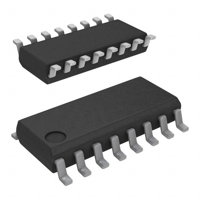
Consulte las especificaciones para obtener detalles del producto.

SN74AHC139D
Product Overview
- Category: Integrated Circuit (IC)
- Use: Decoder/Demultiplexer
- Characteristics: High-speed, low-power, dual 2-to-4 line decoder/demultiplexer
- Package: SOIC (Small Outline Integrated Circuit)
- Essence: The SN74AHC139D is a versatile IC that can be used as both a decoder and a demultiplexer. It provides high-speed operation while consuming low power.
- Packaging/Quantity: The SN74AHC139D is available in a standard SOIC package and is typically sold in reels of 2500 units.
Specifications
- Supply Voltage Range: 2V to 5.5V
- High-Level Input Voltage: 2V to VCC + 0.5V
- Low-Level Input Voltage: -0.5V to 0.8V
- High-Level Output Current: -8mA
- Low-Level Output Current: 8mA
- Operating Temperature Range: -40°C to 85°C
Detailed Pin Configuration
The SN74AHC139D has a total of 16 pins. Here is the detailed pin configuration:
- A0: Address input 0
- A1: Address input 1
- G1: Enable input 1
- Y0: Output 0
- Y1: Output 1
- G2A: Enable input 2A
- Y2: Output 2
- Y3: Output 3
- GND: Ground
- Y4: Output 4
- Y5: Output 5
- G2B: Enable input 2B
- Y6: Output 6
- Y7: Output 7
- VCC: Supply voltage
- NC: Not connected
Functional Features
- Dual 2-to-4 line decoder/demultiplexer functionality
- High-speed operation with minimal propagation delay
- Low power consumption, making it suitable for battery-powered devices
- Wide supply voltage range allows compatibility with various systems
- Schmitt-trigger inputs for improved noise immunity
- ESD protection on all inputs and outputs
Advantages and Disadvantages
Advantages: - Versatile IC that can be used as both a decoder and a demultiplexer - High-speed operation ensures efficient data processing - Low power consumption extends battery life in portable devices - Wide supply voltage range provides flexibility in system design - Schmitt-trigger inputs enhance noise immunity - ESD protection safeguards against electrostatic discharge
Disadvantages: - Limited number of output lines (8) may not be sufficient for complex applications requiring more outputs - SOIC package may not be suitable for space-constrained designs
Working Principles
The SN74AHC139D operates based on the principles of digital logic. It takes two address inputs (A0 and A1) and two enable inputs (G1 and G2) to decode or demultiplex the input signals. The selected output line(s) correspond to the binary value of the address inputs. The enable inputs control the activation of the decoder or demultiplexer.
Detailed Application Field Plans
The SN74AHC139D finds applications in various fields, including:
- Data decoding in microcontrollers and digital systems
- Address decoding in memory systems
- Signal routing and selection in communication systems
- Multiplexing and demultiplexing in data transmission
- Control signal generation in industrial automation
Detailed and Complete Alternative Models
Here are some alternative models that offer similar functionality to the SN74AHC139D:
- 74HC139: High-speed CMOS logic dual 2-to-4 line decoder/demultiplexer
- CD74HC139: High-speed CMOS logic dual 2-to-4 line decoder/demultiplexer
- MC74HC139: High-speed CMOS logic dual 2-to-4 line decoder/demultiplexer
These alternative models are widely available and can be used as substitutes for the SN74AHC139D in various applications.
Word count: 527 words
Enumere 10 preguntas y respuestas comunes relacionadas con la aplicación de SN74AHC139D en soluciones técnicas
Sure! Here are 10 common questions and answers related to the application of SN74AHC139D in technical solutions:
Q: What is SN74AHC139D? A: SN74AHC139D is a dual 2-to-4 line decoder/demultiplexer integrated circuit (IC) that can be used in various digital logic applications.
Q: What is the purpose of SN74AHC139D? A: SN74AHC139D is designed to convert binary information from a two-bit input into four separate output lines, making it useful for address decoding, data routing, and signal demultiplexing.
Q: What is the voltage range supported by SN74AHC139D? A: SN74AHC139D operates within a voltage range of 2V to 5.5V, making it compatible with both 3.3V and 5V systems.
Q: How many inputs does SN74AHC139D have? A: SN74AHC139D has two independent 2-input decoders, allowing you to control up to four output lines.
Q: Can SN74AHC139D be cascaded to increase the number of outputs? A: Yes, multiple SN74AHC139D ICs can be cascaded together to increase the number of output lines by connecting the enable (E) pin of the subsequent IC to the output of the previous IC.
Q: What is the maximum frequency at which SN74AHC139D can operate? A: SN74AHC139D has a maximum operating frequency of 50 MHz, making it suitable for high-speed digital applications.
Q: Does SN74AHC139D have any built-in protection features? A: Yes, SN74AHC139D has built-in diode protection on all inputs and outputs, providing protection against electrostatic discharge (ESD) and other voltage spikes.
Q: Can SN74AHC139D be used in both active-high and active-low applications? A: Yes, SN74AHC139D supports both active-high and active-low enable inputs, allowing flexibility in designing different logic configurations.
Q: What is the power supply requirement for SN74AHC139D? A: SN74AHC139D requires a single power supply voltage (VCC) between 2V and 5.5V, making it compatible with standard digital logic power supplies.
Q: Are there any specific application notes or reference designs available for SN74AHC139D? A: Yes, Texas Instruments provides detailed application notes and reference designs in the datasheet of SN74AHC139D, which can help you understand its usage in various technical solutions.
Please note that these answers are general and may vary depending on the specific implementation and requirements of your technical solution.

