Consulte las especificaciones para obtener detalles del producto.

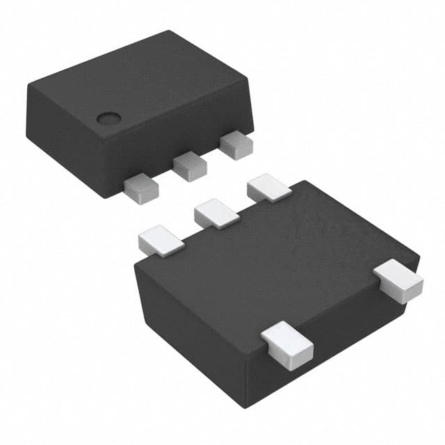
SN74AUC1G02DRLR
Product Overview
- Category: Integrated Circuit
- Use: Logic Gate
- Characteristics: Single 2-Input NOR Gate
- Package: SOT-553
- Essence: High-Speed CMOS Technology
- Packaging/Quantity: Tape and Reel, 3000 pieces per reel
Specifications
- Logic Family: AUC
- Number of Inputs: 2
- Number of Outputs: 1
- Supply Voltage Range: 0.8V to 3.6V
- Operating Temperature Range: -40°C to +85°C
- Propagation Delay: 2.5ns (typical)
- Output Drive Capability: ±24mA at 3.3V
- Power Dissipation: 4.5mW (typical)
Detailed Pin Configuration
The SN74AUC1G02DRLR has a total of 5 pins:
- Pin 1: Input A
- Pin 2: Input B
- Pin 3: Ground (GND)
- Pin 4: Output Y
- Pin 5: Power Supply (VCC)
Functional Features
- High-speed operation due to advanced CMOS technology
- Low power consumption
- Wide supply voltage range for compatibility with various systems
- Schmitt-trigger input allows for noise immunity
- Small package size for space-constrained applications
Advantages and Disadvantages
Advantages: - High-speed performance enables efficient data processing - Low power consumption reduces energy usage - Wide supply voltage range enhances versatility - Noise immunity provided by the Schmitt-trigger input ensures reliable operation - Compact package size allows for flexible integration in small designs
Disadvantages: - Limited number of inputs and outputs restricts complex logic operations - Not suitable for high-voltage applications
Working Principles
The SN74AUC1G02DRLR is a single 2-input NOR gate that operates using high-speed CMOS technology. It accepts two input signals, A and B, and produces an output signal, Y, based on the NOR logic function. The gate utilizes a Schmitt-trigger input, which provides noise immunity by ensuring stable switching thresholds even in the presence of input voltage fluctuations.
Detailed Application Field Plans
The SN74AUC1G02DRLR can be used in various applications, including but not limited to:
- Digital logic circuits
- Microcontrollers
- Data communication systems
- Industrial automation
- Consumer electronics
Detailed and Complete Alternative Models
- SN74AUC1G00DRLR: Single 2-Input NAND Gate
- SN74AUC1G04DRLR: Single Inverter Gate
- SN74AUC2G02DRLR: Dual 2-Input NOR Gate
- SN74AUC2G04DRLR: Dual Inverter Gate
- SN74AUC3G02DRLR: Triple 2-Input NOR Gate
These alternative models offer similar functionality and characteristics, providing flexibility in choosing the most suitable option for specific design requirements.
Word count: 346 words
Enumere 10 preguntas y respuestas comunes relacionadas con la aplicación de SN74AUC1G02DRLR en soluciones técnicas
Sure! Here are 10 common questions and answers related to the application of SN74AUC1G02DRLR in technical solutions:
Q1: What is SN74AUC1G02DRLR? A1: SN74AUC1G02DRLR is a single 2-input positive-NOR gate IC (integrated circuit) that is commonly used in digital logic circuits.
Q2: What is the voltage supply range for SN74AUC1G02DRLR? A2: The voltage supply range for SN74AUC1G02DRLR is typically between 0.8V and 3.6V.
Q3: What is the maximum output current of SN74AUC1G02DRLR? A3: The maximum output current of SN74AUC1G02DRLR is around 32mA.
Q4: Can SN74AUC1G02DRLR be used in battery-powered applications? A4: Yes, SN74AUC1G02DRLR can be used in battery-powered applications due to its low power consumption and wide voltage supply range.
Q5: What is the operating temperature range for SN74AUC1G02DRLR? A5: The operating temperature range for SN74AUC1G02DRLR is typically between -40°C and 85°C.
Q6: How many inputs does SN74AUC1G02DRLR have? A6: SN74AUC1G02DRLR has 2 inputs.
Q7: What is the typical propagation delay of SN74AUC1G02DRLR? A7: The typical propagation delay of SN74AUC1G02DRLR is around 2.9ns.
Q8: Can SN74AUC1G02DRLR be used in high-speed applications? A8: Yes, SN74AUC1G02DRLR can be used in high-speed applications due to its low propagation delay and fast switching characteristics.
Q9: Is SN74AUC1G02DRLR compatible with other logic families? A9: Yes, SN74AUC1G02DRLR is compatible with a wide range of logic families, including CMOS, TTL, and LVTTL.
Q10: What are some common applications of SN74AUC1G02DRLR? A10: Some common applications of SN74AUC1G02DRLR include signal inversion, logic level conversion, and general-purpose digital logic circuits.
Please note that the answers provided here are general and may vary depending on specific datasheet specifications and application requirements.

