

Consulte las especificaciones para obtener detalles del producto.
SN74AUP1G125YZTR
Product Overview
- Category: Integrated Circuit
- Use: Buffer/Driver
- Characteristics: Single Gate, Non-Inverting, Tri-State
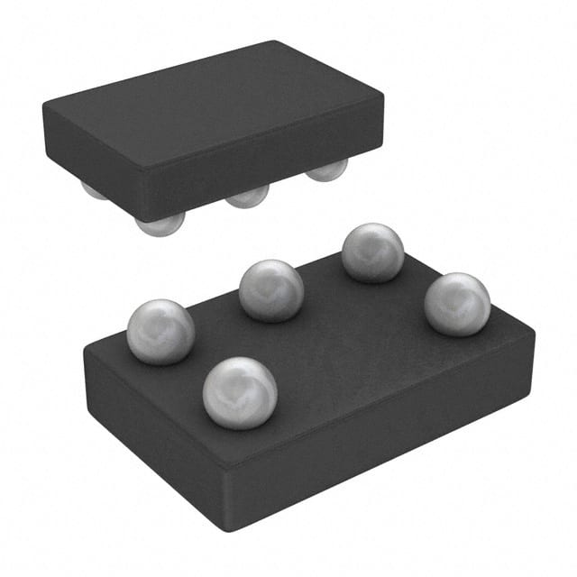
- Package: SOT-553
- Essence: High-Speed CMOS Logic
- Packaging/Quantity: Tape and Reel, 3000 pieces per reel
Specifications
- Supply Voltage Range: 0.8V to 3.6V
- Input Voltage Range: 0V to VCC
- Output Voltage Range: 0V to VCC
- Maximum Operating Frequency: 500MHz
- Propagation Delay: 2.5ns (typical)
- Output Drive Capability: ±24mA
- Operating Temperature Range: -40°C to +85°C
Detailed Pin Configuration
The SN74AUP1G125YZTR has a total of 5 pins:
- GND (Ground): Connected to the ground reference of the circuit.
- VCC (Supply Voltage): Connected to the positive supply voltage.
- OE (Output Enable): Controls the tri-state output buffer.
- A (Input): Data input pin.
- Y (Output): Buffered output pin.
Functional Features
- Single gate buffer/driver with non-inverting functionality.
- Tri-state output allows for high impedance state when disabled.
- High-speed operation suitable for various applications.
- Wide supply voltage range enables compatibility with different systems.
- Low power consumption for energy-efficient designs.
Advantages and Disadvantages
Advantages: - Small package size saves board space. - High-speed operation enables fast data transmission. - Tri-state output provides flexibility in bus sharing applications. - Wide supply voltage range allows for compatibility with different voltage levels.
Disadvantages: - Limited output drive capability may not be suitable for high-current applications. - Single gate design limits the number of inputs/outputs.
Working Principles
The SN74AUP1G125YZTR is a single gate buffer/driver that amplifies and buffers digital signals. It operates using high-speed CMOS logic, allowing for fast data transmission. The non-inverting functionality ensures that the output signal matches the input signal. The tri-state feature allows the output to be in a high impedance state when disabled, enabling multiple devices to share a common bus.
Detailed Application Field Plans
The SN74AUP1G125YZTR can be used in various applications, including but not limited to: - Communication systems - Data storage devices - Industrial automation - Consumer electronics - Automotive electronics - Medical equipment
Detailed and Complete Alternative Models
Some alternative models that offer similar functionality to the SN74AUP1G125YZTR include: - SN74LVC1G125DBVR - SN74LV1T125DBVR - SN74AHC1G125DBVR - SN74AHCT1G125DBVR - SN74LVC1G125DCKR
These alternatives may have different package options, voltage ranges, or other specifications, but they serve the same purpose as the SN74AUP1G125YZTR.
Word count: 311
Enumere 10 preguntas y respuestas comunes relacionadas con la aplicación de SN74AUP1G125YZTR en soluciones técnicas
Sure! Here are 10 common questions and answers related to the application of SN74AUP1G125YZTR in technical solutions:
Q1: What is the SN74AUP1G125YZTR? A1: The SN74AUP1G125YZTR is a single bus buffer gate with 3-state output. It is commonly used in digital logic circuits for signal buffering and level shifting.
Q2: What is the operating voltage range of SN74AUP1G125YZTR? A2: The operating voltage range of SN74AUP1G125YZTR is from 0.8V to 3.6V.
Q3: What is the maximum output current of SN74AUP1G125YZTR? A3: The maximum output current of SN74AUP1G125YZTR is typically 32mA.
Q4: Can SN74AUP1G125YZTR be used as a level shifter? A4: Yes, SN74AUP1G125YZTR can be used as a level shifter to convert signals between different voltage levels.
Q5: What is the propagation delay of SN74AUP1G125YZTR? A5: The propagation delay of SN74AUP1G125YZTR is typically around 2.7ns.
Q6: Is SN74AUP1G125YZTR compatible with other logic families? A6: Yes, SN74AUP1G125YZTR is compatible with various logic families such as CMOS, TTL, and LVCMOS.
Q7: Can SN74AUP1G125YZTR drive capacitive loads? A7: Yes, SN74AUP1G125YZTR can drive small capacitive loads up to a certain limit specified in the datasheet.
Q8: What is the package type of SN74AUP1G125YZTR? A8: SN74AUP1G125YZTR is available in a small SOT-23-5 package.
Q9: Can SN74AUP1G125YZTR be used in battery-powered applications? A9: Yes, SN74AUP1G125YZTR is suitable for battery-powered applications due to its low power consumption.
Q10: Are there any recommended decoupling capacitors for SN74AUP1G125YZTR? A10: It is generally recommended to use a 0.1µF ceramic capacitor placed close to the VCC and GND pins of SN74AUP1G125YZTR for proper decoupling.
Please note that these answers are general and it's always important to refer to the specific datasheet and application notes for accurate information and guidelines.