

Consulte las especificaciones para obtener detalles del producto.
SN74AUP1G34DRYR
Product Overview
- Category: Integrated Circuit
- Use: Logic Gate
- Characteristics: Single Schmitt-Trigger Buffer
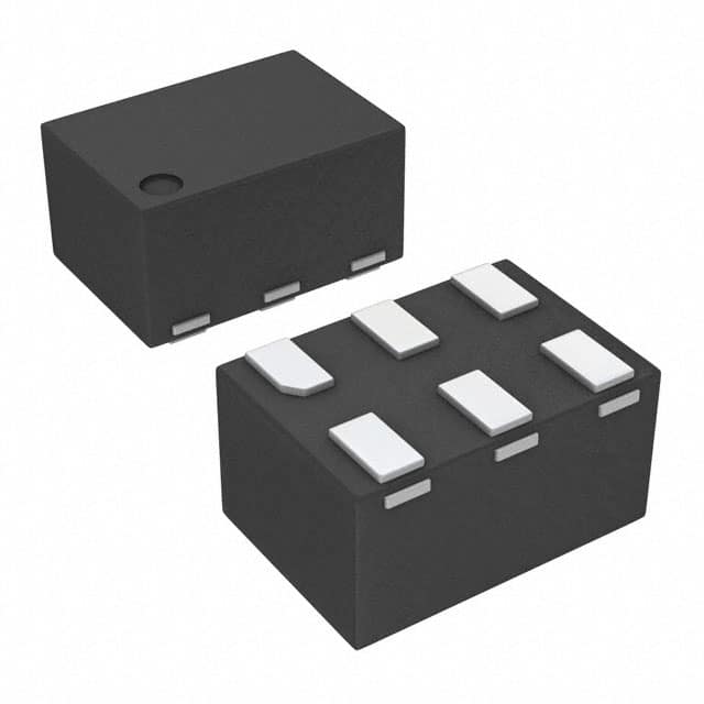
- Package: SOT-23-5
- Essence: High-speed, low-power consumption buffer
- Packaging/Quantity: Tape and Reel, 3000 pieces per reel
Specifications
- Supply Voltage Range: 0.8V to 3.6V
- Input Voltage Range: -0.5V to VCC + 0.5V
- Output Voltage Range: 0V to VCC
- Maximum Operating Frequency: 500MHz
- Propagation Delay: 2.7ns (typical)
- Input Capacitance: 1.5pF (typical)
- Output Current: ±4mA
Detailed Pin Configuration
The SN74AUP1G34DRYR has a total of five pins arranged as follows:
____
   VCC|    |GND
   IN |    |OUT
      |____|
- VCC: Power supply pin (+)
- GND: Ground pin (-)
- IN: Input pin
- OUT: Output pin
Functional Features
- Single Schmitt-trigger buffer with open-drain output
- Provides hysteresis for improved noise immunity
- Supports bidirectional level translation
- Low power consumption
- High-speed operation
Advantages and Disadvantages
Advantages: - High-speed operation allows for efficient signal processing - Low power consumption extends battery life in portable devices - Hysteresis improves noise immunity, ensuring reliable operation - Bidirectional level translation enables compatibility between different voltage domains
Disadvantages: - Limited output current may restrict use in certain applications requiring higher drive capability - Small package size may pose challenges for manual soldering or handling
Working Principles
The SN74AUP1G34DRYR is a single Schmitt-trigger buffer that operates as a voltage level translator. It accepts a digital input signal and provides an output signal with improved noise immunity. The Schmitt-trigger input stage introduces hysteresis, which helps to eliminate noise-induced false triggering.
The device operates within a wide supply voltage range of 0.8V to 3.6V, making it suitable for various low-power applications. It features a high-speed operation with a maximum frequency of 500MHz, enabling efficient signal processing.
Detailed Application Field Plans
The SN74AUP1G34DRYR can be used in a wide range of applications, including but not limited to:
- Battery-powered devices: Due to its low power consumption, the IC is ideal for use in portable electronics such as smartphones, tablets, and wearables.
- Communication systems: The high-speed operation makes it suitable for signal conditioning and level shifting in communication interfaces like UART, I2C, and SPI.
- Industrial automation: The device can be utilized in control systems, sensors, and actuators, providing reliable signal buffering and level translation.
- Automotive electronics: With its ability to operate at low voltages, the IC finds application in automotive systems, including infotainment, lighting, and body control modules.
Detailed and Complete Alternative Models
- SN74AUP1G34DCKR: Similar specifications and functionality, but available in SC-70 package.
- SN74LVC1G34DBVR: Low-voltage CMOS buffer with similar characteristics, available in SOT-23-5 package.
- SN74HCT1G34DCKR: High-speed CMOS buffer with comparable specifications, available in SC-70 package.
These alternative models offer similar functionality and can be used as replacements for the SN74AUP1G34DRYR in various applications.
Word count: 511 words
Enumere 10 preguntas y respuestas comunes relacionadas con la aplicación de SN74AUP1G34DRYR en soluciones técnicas
Sure! Here are 10 common questions and answers related to the application of SN74AUP1G34DRYR in technical solutions:
Q1: What is SN74AUP1G34DRYR? A1: SN74AUP1G34DRYR is a single buffer gate IC (integrated circuit) that provides high-performance voltage translation from a low-voltage (LVCMOS/LVTTL) input signal to a higher voltage (up to 5.5V) output signal.
Q2: What is the typical application of SN74AUP1G34DRYR? A2: SN74AUP1G34DRYR is commonly used for level shifting applications, where it enables communication between devices operating at different voltage levels.
Q3: What is the maximum voltage level that SN74AUP1G34DRYR can handle? A3: SN74AUP1G34DRYR can handle a maximum voltage level of 5.5V.
Q4: What is the input voltage range for SN74AUP1G34DRYR? A4: The input voltage range for SN74AUP1G34DRYR is typically between 0V and 3.6V.
Q5: What is the output voltage range for SN74AUP1G34DRYR? A5: The output voltage range for SN74AUP1G34DRYR is typically between 0V and 5.5V.
Q6: Can SN74AUP1G34DRYR be used for bidirectional level shifting? A6: No, SN74AUP1G34DRYR is a unidirectional buffer gate and cannot be used for bidirectional level shifting.
Q7: What is the maximum data rate supported by SN74AUP1G34DRYR? A7: SN74AUP1G34DRYR can support data rates up to 100 MHz.
Q8: Does SN74AUP1G34DRYR have any built-in protection features? A8: Yes, SN74AUP1G34DRYR has built-in ESD (electrostatic discharge) protection to safeguard against electrostatic damage during handling and operation.
Q9: Can SN74AUP1G34DRYR be used in battery-powered applications? A9: Yes, SN74AUP1G34DRYR is suitable for battery-powered applications as it operates at low power supply voltages.
Q10: What package options are available for SN74AUP1G34DRYR? A10: SN74AUP1G34DRYR is available in various package options, including SOT-23 and X2SON, providing flexibility for different PCB layouts and space constraints.
Please note that these answers are general and may vary depending on specific datasheet specifications and application requirements.