

Consulte las especificaciones para obtener detalles del producto.
SN74FB2033ARCRG3
Product Overview
- Category: Integrated Circuit
- Use: Logic Gate
- Characteristics: High-speed, Low-power consumption
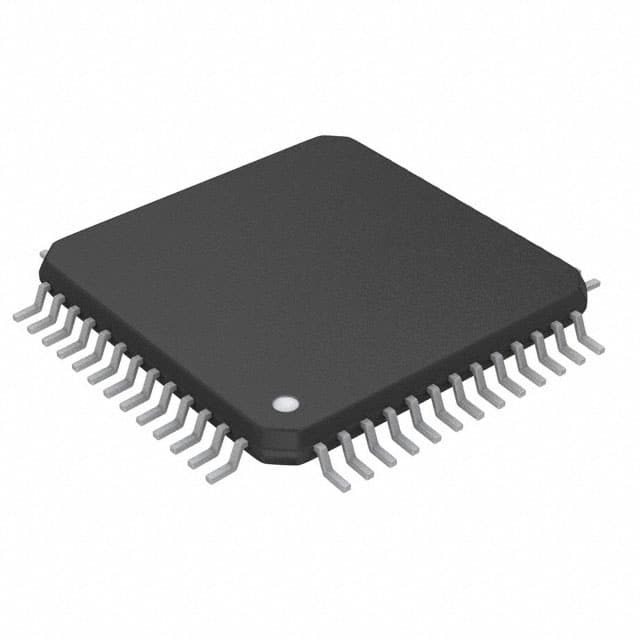
- Package: QFN (Quad Flat No-leads)
- Essence: Digital Buffer/Driver
- Packaging/Quantity: Tape and Reel, 2500 units per reel
Specifications
- Supply Voltage Range: 1.65V to 3.6V
- Input Voltage Range: 0V to VCC
- Output Voltage Range: 0V to VCC
- Operating Temperature Range: -40°C to +85°C
- Propagation Delay Time: 2.5ns (typical)
- Output Drive Capability: ±24mA
Detailed Pin Configuration
The SN74FB2033ARCRG3 has a total of 16 pins arranged as follows:
```
| | --| U1 |-- |___________|
Pin Configuration: 1. A1 2. B1 3. Y1 4. GND 5. A2 6. B2 7. Y2 8. VCC 9. A3 10. B3 11. Y3 12. GND 13. A4 14. B4 15. Y4 16. VCC ```
Functional Features
- High-speed operation allows for efficient data processing.
- Low-power consumption ensures energy efficiency.
- Wide supply voltage range enables compatibility with various systems.
- Output drive capability allows for driving external loads.
Advantages and Disadvantages
Advantages: - High-speed operation enhances system performance. - Low-power consumption prolongs battery life in portable devices. - Wide supply voltage range provides flexibility in system design. - Output drive capability enables direct connection to external devices.
Disadvantages: - Limited number of input/output channels. - Not suitable for applications requiring complex logic functions.
Working Principles
The SN74FB2033ARCRG3 is a digital buffer/driver integrated circuit that amplifies and buffers digital signals. It operates by receiving input signals (A1-A4, B1-B4) and producing corresponding output signals (Y1-Y4). The device uses CMOS technology, allowing for high-speed operation and low-power consumption.
Detailed Application Field Plans
The SN74FB2033ARCRG3 is commonly used in various digital systems, including:
- Microcontrollers: Provides signal buffering and driving capabilities for interfacing with external devices.
- Communication Systems: Facilitates signal transmission between different components in communication networks.
- Industrial Automation: Enables efficient data processing and control in automated systems.
- Consumer Electronics: Supports signal amplification and driving in devices such as smartphones and tablets.
Detailed and Complete Alternative Models
- SN74LVC1G07DBVR
- SN74LVC1G07DCKR
- SN74LVC1G07DRLR
- SN74LVC1G07YZPR
- SN74LVC1G07YZTR
These alternative models offer similar functionality and characteristics to the SN74FB2033ARCRG3, providing options for different design requirements.
Word count: 345 words
Enumere 10 preguntas y respuestas comunes relacionadas con la aplicación de SN74FB2033ARCRG3 en soluciones técnicas
Sure! Here are 10 common questions and answers related to the application of SN74FB2033ARCRG3 in technical solutions:
Q: What is SN74FB2033ARCRG3? A: SN74FB2033ARCRG3 is a specific model of integrated circuit (IC) manufactured by Texas Instruments.
Q: What is the purpose of SN74FB2033ARCRG3? A: SN74FB2033ARCRG3 is a dual supply voltage level translator IC used for bidirectional voltage translation between two different voltage domains.
Q: What voltage levels can SN74FB2033ARCRG3 translate between? A: SN74FB2033ARCRG3 can translate between voltage levels of 1.2V and 3.6V.
Q: How many channels does SN74FB2033ARCRG3 have? A: SN74FB2033ARCRG3 has 2 channels, allowing bidirectional translation for two separate signals.
Q: What is the maximum data rate supported by SN74FB2033ARCRG3? A: SN74FB2033ARCRG3 supports a maximum data rate of 100 Mbps.
Q: Can SN74FB2033ARCRG3 be used in both directions simultaneously? A: Yes, SN74FB2033ARCRG3 supports simultaneous bidirectional translation.
Q: Is SN74FB2033ARCRG3 suitable for level shifting between different logic families? A: Yes, SN74FB2033ARCRG3 can be used for level shifting between various logic families such as TTL, CMOS, and LVCMOS.
Q: Does SN74FB2033ARCRG3 require external components for operation? A: Yes, SN74FB2033ARCRG3 requires external pull-up resistors and decoupling capacitors for proper operation.
Q: What is the operating temperature range of SN74FB2033ARCRG3? A: SN74FB2033ARCRG3 can operate within a temperature range of -40°C to +85°C.
Q: Where can I find more information about using SN74FB2033ARCRG3 in my technical solution? A: You can refer to the datasheet provided by Texas Instruments or visit their official website for detailed application notes and guidelines.
Please note that the answers provided here are general and may vary depending on specific use cases and requirements. It is always recommended to consult the datasheet and relevant technical documentation for accurate information.