

Consulte las especificaciones para obtener detalles del producto.
SN74FB2040RCR
Product Overview
- Category: Integrated Circuit (IC)
- Use: Logic Gate
- Characteristics: High-speed, Low-power consumption
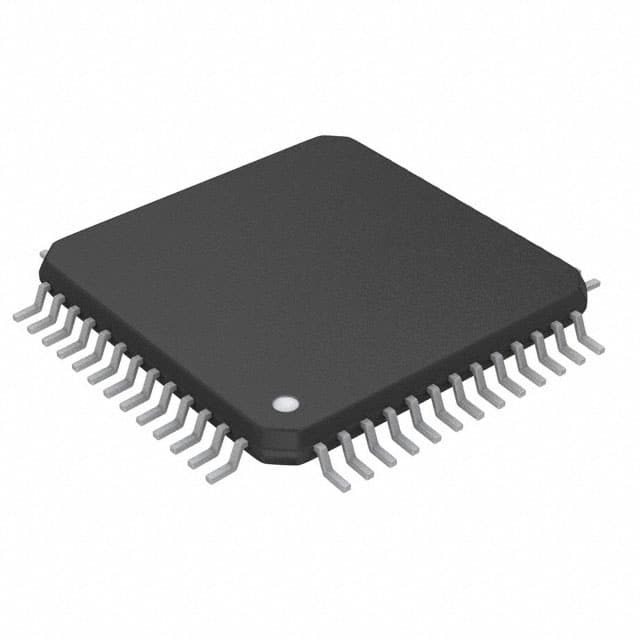
- Package: QFN (Quad Flat No-leads)
- Essence: Digital Logic IC
- Packaging/Quantity: Tape and Reel, 2500 units per reel
Specifications
- Supply Voltage: 1.65V to 3.6V
- Logic Family: FB (Fast Buffer)
- Number of Inputs: 4
- Number of Outputs: 4
- Propagation Delay: 2.5ns (typical)
- Operating Temperature Range: -40°C to +85°C
Detailed Pin Configuration
The SN74FB2040RCR has a total of 16 pins arranged in a QFN package. The pin configuration is as follows:
Pin 1: Output Y1
Pin 2: Input A1
Pin 3: Input B1
Pin 4: GND
Pin 5: Output Y2
Pin 6: Input A2
Pin 7: Input B2
Pin 8: VCC
Pin 9: Output Y3
Pin 10: Input A3
Pin 11: Input B3
Pin 12: NC (No Connection)
Pin 13: Output Y4
Pin 14: Input A4
Pin 15: Input B4
Pin 16: GND
Functional Features
- High-speed operation allows for efficient data processing.
- Low-power consumption makes it suitable for battery-powered devices.
- Four independent logic gates provide flexibility in circuit design.
- Wide operating voltage range enables compatibility with various systems.
Advantages and Disadvantages
Advantages: - High-speed performance enhances overall system efficiency. - Low-power consumption prolongs battery life in portable devices. - Compact QFN package saves board space. - Wide operating voltage range allows for versatile applications.
Disadvantages: - Limited number of inputs and outputs may restrict complex circuit designs. - Propagation delay may affect real-time applications with strict timing requirements.
Working Principles
The SN74FB2040RCR is a digital logic IC that operates based on the principles of Boolean algebra. It consists of four independent logic gates, each capable of performing logical operations on binary inputs (A and B) and producing an output (Y). The gates utilize transistor-based switching circuits to implement various logic functions such as AND, OR, and XOR.
Detailed Application Field Plans
The SN74FB2040RCR finds applications in various fields, including:
- Consumer Electronics: Used in smartphones, tablets, and gaming consoles for signal processing and control logic.
- Automotive: Integrated into automotive systems for data communication, sensor interfacing, and control functions.
- Industrial Automation: Employed in industrial control systems for logic operations, signal conditioning, and interface circuitry.
- Communication Systems: Utilized in networking equipment, routers, and switches for data routing and protocol handling.
Detailed and Complete Alternative Models
- SN74LVC1G04DBVR: Single Inverter Gate, SOT-23 package
- SN74HC08N: Quad 2-Input AND Gate, DIP-14 package
- SN74LS32N: Quad 2-Input OR Gate, DIP-14 package
- SN74LVX245DWR: Octal Bus Transceiver, SOIC-20 package
- SN74ACT244DW: Octal Buffer/Line Driver, SOIC-20 package
These alternative models offer similar functionality and can be considered as substitutes for the SN74FB2040RCR in different applications.
Word count: 410
Enumere 10 preguntas y respuestas comunes relacionadas con la aplicación de SN74FB2040RCR en soluciones técnicas
Sure! Here are 10 common questions and answers related to the application of SN74FB2040RCR in technical solutions:
1. What is SN74FB2040RCR? SN74FB2040RCR is a specific model of integrated circuit (IC) manufactured by Texas Instruments. It is a high-speed, low-power, 20-bit configurable registered buffer with parity.
2. What is the purpose of SN74FB2040RCR? The purpose of SN74FB2040RCR is to provide buffering and parity generation/checking capabilities for digital signals in various electronic systems.
3. What are the key features of SN74FB2040RCR? Some key features of SN74FB2040RCR include configurable I/O voltage levels, selectable output drive strength, programmable input/output delays, and built-in parity generation/checking.
4. What are the typical applications of SN74FB2040RCR? SN74FB2040RCR can be used in a wide range of applications such as memory subsystems, data communication systems, industrial automation, and embedded systems where signal buffering and parity checking are required.
5. What is the operating voltage range of SN74FB2040RCR? SN74FB2040RCR operates within a voltage range of 1.65V to 3.6V.
6. How many I/O pins does SN74FB2040RCR have? SN74FB2040RCR has a total of 20 I/O pins.
7. Can SN74FB2040RCR operate at high speeds? Yes, SN74FB2040RCR is designed to operate at high speeds, with a maximum toggle frequency of 400 MHz.
8. Does SN74FB2040RCR support different output drive strengths? Yes, SN74FB2040RCR supports selectable output drive strengths, allowing flexibility in driving different loads.
9. Can SN74FB2040RCR be used in both input and output modes? Yes, SN74FB2040RCR can be configured to operate in both input and output modes, depending on the specific requirements of the application.
10. Does SN74FB2040RCR have built-in parity generation/checking? Yes, SN74FB2040RCR has built-in parity generation and checking capabilities, which can be enabled or disabled based on the application's needs.
Please note that these questions and answers are general and may vary depending on the specific implementation and usage of SN74FB2040RCR in different technical solutions.