Consulte las especificaciones para obtener detalles del producto.

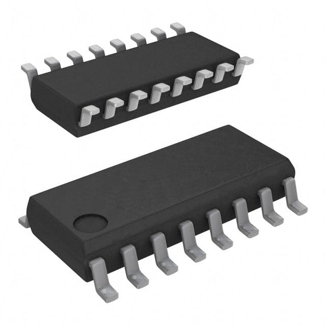
SN74HC253DRG4
Product Overview
- Category: Integrated Circuit (IC)
- Use: Multiplexer/Demultiplexer
- Characteristics: High-speed, low-power consumption
- Package: SOIC (Small Outline Integrated Circuit)
- Essence: Dual 4-to-1 multiplexer/demultiplexer
- Packaging/Quantity: Tape and Reel, 2500 units per reel
Specifications
- Supply Voltage Range: 2V to 6V
- Input Voltage Range: 0V to VCC
- Output Voltage Range: 0V to VCC
- Operating Temperature Range: -40°C to +85°C
- Propagation Delay Time: 10 ns (typical)
- Maximum Quiescent Current: 8 μA
- Maximum Operating Frequency: 50 MHz
Pin Configuration
The SN74HC253DRG4 has a total of 16 pins. The pin configuration is as follows:
__    __
   A1 -| 1    16 |- VCC
   B1 -| 2    15 |- A2
   C1 -| 3    14 |- B2
   D1 -| 4    13 |- C2
   D2 -| 5    12 |- D2
   C2 -| 6    11 |- D1
   B2 -| 7    10 |- C1
   A2 -| 8     9 |- B1
       |________|
Functional Features
- Dual 4-to-1 multiplexer/demultiplexer functionality
- Can be used as a data selector or data distributor
- High-speed operation allows for efficient data transmission
- Low-power consumption makes it suitable for battery-powered devices
- Wide supply voltage range provides flexibility in various applications
Advantages and Disadvantages
Advantages
- High-speed operation enables quick data processing
- Low-power consumption prolongs battery life
- Wide supply voltage range allows for versatile use
- Compact SOIC package saves board space
Disadvantages
- Limited number of input/output channels
- Propagation delay may affect real-time applications
Working Principles
The SN74HC253DRG4 is a dual 4-to-1 multiplexer/demultiplexer IC. It can select one of the four inputs and route it to the output based on the control inputs. In multiplexer mode, the selected input is transmitted to the output, while in demultiplexer mode, the input is distributed to one of the four outputs.
The IC operates by utilizing logic gates and flip-flops to control the routing of data. The inputs are decoded to determine the desired output channel, and the internal circuitry ensures that only the selected input is propagated to the output.
Detailed Application Field Plans
The SN74HC253DRG4 finds applications in various fields, including:
- Data communication systems: Used for data selection and distribution in multiplexed communication channels.
- Digital signal processing: Enables efficient data routing in DSP algorithms.
- Industrial automation: Facilitates data selection and distribution in control systems.
- Consumer electronics: Utilized in devices requiring multiple input/output channels, such as audio/video equipment.
- Automotive electronics: Enables data routing in automotive control modules.
Detailed and Complete Alternative Models
- CD74HC253E: Similar functionality with a different package (DIP-16).
- MC74HC253N: Equivalent functionality with a different package (PDIP-16).
- SN54HC253J: Comparable features with a different package (CDIP-16).
These alternative models provide similar functionality to the SN74HC253DRG4 and can be used as replacements in various applications.
Word count: 498 words
Enumere 10 preguntas y respuestas comunes relacionadas con la aplicación de SN74HC253DRG4 en soluciones técnicas
Sure! Here are 10 common questions and answers related to the application of SN74HC253DRG4 in technical solutions:
Q: What is SN74HC253DRG4? A: SN74HC253DRG4 is a dual 4-to-1 multiplexer/demultiplexer integrated circuit (IC) that can be used in various digital applications.
Q: What is the purpose of SN74HC253DRG4? A: SN74HC253DRG4 allows you to select one of four input signals and route it to an output, or vice versa, based on control inputs.
Q: What voltage levels does SN74HC253DRG4 support? A: SN74HC253DRG4 operates at a voltage range of 2V to 6V, making it compatible with both TTL and CMOS logic families.
Q: How many control inputs does SN74HC253DRG4 have? A: SN74HC253DRG4 has two control inputs, which determine the routing of the input signals to the outputs.
Q: Can SN74HC253DRG4 be used as a demultiplexer? A: Yes, SN74HC253DRG4 can function as a demultiplexer by using its control inputs to select one of the four outputs for routing the input signal.
Q: How much current can SN74HC253DRG4 source or sink? A: SN74HC253DRG4 can source or sink up to 4mA of current per output pin, making it suitable for driving standard logic gates.
Q: Is SN74HC253DRG4 compatible with 5V logic systems? A: Yes, SN74HC253DRG4 is compatible with 5V logic systems, as it can operate within the voltage range of 2V to 6V.
Q: Can SN74HC253DRG4 be cascaded to increase the number of inputs or outputs? A: Yes, multiple SN74HC253DRG4 ICs can be cascaded together to increase the number of inputs or outputs in a digital circuit.
Q: What is the maximum operating frequency of SN74HC253DRG4? A: SN74HC253DRG4 has a maximum operating frequency of 50MHz, making it suitable for high-speed digital applications.
Q: Are there any special considerations when using SN74HC253DRG4? A: It is important to ensure that the power supply and ground connections are properly decoupled to minimize noise and ensure reliable operation.
Please note that these answers are general and may vary depending on specific application requirements.

