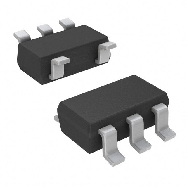
Consulte las especificaciones para obtener detalles del producto.

SN74LVC1G04DCKT
Product Overview
- Category: Integrated Circuit (IC)
- Use: Logic Gate
- Characteristics: Single Inverter Gate, Low Voltage, CMOS Technology
- Package: SC-70 (SOT-323), 5-Pin
- Essence: The SN74LVC1G04DCKT is a single inverter gate IC that operates at low voltage levels. It is designed using complementary metal-oxide-semiconductor (CMOS) technology.
- Packaging/Quantity: The SN74LVC1G04DCKT is available in tape and reel packaging, with 3000 units per reel.
Specifications
- Supply Voltage Range: 1.65V to 5.5V
- Input Voltage Range: 0V to VCC
- Output Voltage Range: 0V to VCC
- Operating Temperature Range: -40°C to +125°C
- Propagation Delay: 4.3ns (typical) at 3.3V supply voltage
- Input Capacitance: 2pF (typical)
- Output Drive Capability: ±24mA
Detailed Pin Configuration
The SN74LVC1G04DCKT has the following pin configuration:
____
   Y --|    |-- VCC
 GND --|    |-- A
      --|____|-- NC
- Y: Output
- VCC: Power Supply
- GND: Ground
- A: Input
- NC: No Connection
Functional Features
- The SN74LVC1G04DCKT is a single inverter gate that provides logic inversion of the input signal.
- It operates at low voltage levels, making it suitable for battery-powered devices.
- The CMOS technology used in its design ensures low power consumption and high noise immunity.
- It has a wide supply voltage range, allowing compatibility with various systems.
Advantages and Disadvantages
Advantages
- Low power consumption
- High noise immunity
- Wide supply voltage range
- Small package size
- Easy integration into circuit designs
Disadvantages
- Limited output drive capability
- Single gate functionality may not be suitable for complex logic operations
Working Principles
The SN74LVC1G04DCKT is based on CMOS technology, which utilizes both NMOS and PMOS transistors to achieve logic functions. In the case of the single inverter gate, the input signal is inverted at the output. When the input is high, the output is low, and vice versa. The CMOS design allows for efficient switching between logic states while consuming minimal power.
Detailed Application Field Plans
The SN74LVC1G04DCKT can be used in various applications, including:
- Battery-powered devices: Due to its low voltage operation and low power consumption, it is suitable for portable electronics such as smartphones, tablets, and wearables.
- Communication systems: It can be used in signal processing circuits, data transmission, and reception modules.
- Industrial automation: The IC can be integrated into control systems, sensors, and actuators for efficient and reliable operation.
- Automotive electronics: It finds application in vehicle control units, infotainment systems, and lighting controls.
- Consumer electronics: It can be utilized in audio/video equipment, gaming consoles, and home automation systems.
Detailed and Complete Alternative Models
- SN74LVC1G04DBVR: SOT-23 package, 3-Pin
- SN74LVC1G04DRLR: X2SON package, 4-Pin
- SN74LVC1G04DRLRG4: X2SON package, 4-Pin (Reel)
These alternative models offer similar functionality and characteristics to the SN74LVC1G04DCKT, but with different package options.
Word count: 511 words
Enumere 10 preguntas y respuestas comunes relacionadas con la aplicación de SN74LVC1G04DCKT en soluciones técnicas
Sure! Here are 10 common questions and answers related to the application of SN74LVC1G04DCKT in technical solutions:
Q1: What is SN74LVC1G04DCKT? A1: SN74LVC1G04DCKT is a single inverter gate IC (Integrated Circuit) that is commonly used in digital logic circuits.
Q2: What is the voltage supply range for SN74LVC1G04DCKT? A2: The voltage supply range for SN74LVC1G04DCKT is typically between 1.65V and 5.5V.
Q3: What is the maximum output current of SN74LVC1G04DCKT? A3: The maximum output current of SN74LVC1G04DCKT is typically around 32mA.
Q4: Can SN74LVC1G04DCKT be used as a level shifter? A4: Yes, SN74LVC1G04DCKT can be used as a level shifter to convert signals from one voltage level to another.
Q5: What is the propagation delay of SN74LVC1G04DCKT? A5: The propagation delay of SN74LVC1G04DCKT is typically around 3.8ns.
Q6: Can SN74LVC1G04DCKT be used in high-speed applications? A6: Yes, SN74LVC1G04DCKT is suitable for high-speed applications due to its low propagation delay.
Q7: Is SN74LVC1G04DCKT compatible with both CMOS and TTL logic levels? A7: Yes, SN74LVC1G04DCKT is compatible with both CMOS and TTL logic levels.
Q8: Can SN74LVC1G04DCKT be used in battery-powered applications? A8: Yes, SN74LVC1G04DCKT is suitable for battery-powered applications due to its low power consumption.
Q9: What is the package type of SN74LVC1G04DCKT? A9: SN74LVC1G04DCKT comes in a small SOT-23 package.
Q10: Can SN74LVC1G04DCKT be used in automotive applications? A10: Yes, SN74LVC1G04DCKT is qualified for automotive applications and can withstand harsh operating conditions.
Please note that the answers provided here are general and may vary depending on specific datasheet specifications and application requirements.

