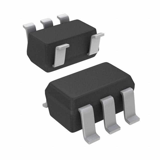
Consulte las especificaciones para obtener detalles del producto.

SN74LVC1G08DBVT
Product Overview
- Category: Integrated Circuit (IC)
- Use: Logic Gate
- Characteristics: Single 2-input AND gate
- Package: SOT-23-5
- Essence: High-speed CMOS technology
- Packaging/Quantity: Tape and Reel, 3000 pieces per reel
Specifications
- Supply Voltage Range: 1.65V to 5.5V
- Input Voltage Range: 0V to VCC
- Output Voltage Range: 0V to VCC
- High-Level Input Voltage: 0.7 x VCC
- Low-Level Input Voltage: 0.3 x VCC
- High-Level Output Voltage: 0.9 x VCC
- Low-Level Output Voltage: 0.1 x VCC
- Propagation Delay: 4.3 ns (typical) at 3.3V
- Operating Temperature Range: -40°C to +85°C
Detailed Pin Configuration
The SN74LVC1G08DBVT has a total of 5 pins:
- GND (Ground): Connected to the ground reference voltage.
- A (Input A): First input for the AND gate.
- B (Input B): Second input for the AND gate.
- Y (Output): Output of the AND gate.
- VCC (Supply Voltage): Connected to the positive supply voltage.
Functional Features
- Single 2-input AND gate functionality.
- Compatible with a wide range of supply voltages.
- High-speed operation due to advanced CMOS technology.
- Low power consumption.
- Schmitt-trigger input allows for hysteresis and noise immunity.
Advantages and Disadvantages
Advantages: - Small package size enables space-saving designs. - Wide supply voltage range allows for compatibility with various systems. - High-speed operation enhances overall system performance. - Low power consumption reduces energy requirements.
Disadvantages: - Limited to a single 2-input AND gate functionality. - Not suitable for applications requiring more complex logic operations.
Working Principles
The SN74LVC1G08DBVT is a single 2-input AND gate that performs logical AND operations on two input signals (A and B). The output (Y) will be high only if both inputs are high; otherwise, the output will be low. The gate operates using high-speed CMOS technology, ensuring fast response times and low power consumption.
Detailed Application Field Plans
The SN74LVC1G08DBVT can be used in various applications, including but not limited to:
- Digital Logic Circuits: It can be utilized as a building block for constructing more complex logic circuits, such as multiplexers, encoders, and adders.
- Microcontrollers and Microprocessors: It can serve as an interface between the microcontroller/microprocessor and other peripheral devices, enabling efficient data processing and control.
- Communication Systems: It can be employed in signal conditioning and data manipulation stages of communication systems, ensuring accurate transmission and reception of digital signals.
- Industrial Automation: It can be integrated into control systems, allowing for logical decision-making and process automation.
Detailed and Complete Alternative Models
- SN74LVC1G00DBVR: Single 2-input NAND gate with similar specifications and package.
- SN74LVC1G32DBVR: Single 2-input OR gate with similar specifications and package.
- SN74LVC1G86DBVR: Single 2-input XOR gate with similar specifications and package.
- SN74LVC1G125DBVR: Single 1-channel buffer/line driver with similar specifications and package.
- SN74LVC1G240DBVR: Single 1-channel inverting buffer/line driver with similar specifications and package.
These alternative models provide similar functionality to the SN74LVC1G08DBVT, allowing users to choose the most suitable option based on their specific requirements.
Word count: 410 words
Enumere 10 preguntas y respuestas comunes relacionadas con la aplicación de SN74LVC1G08DBVT en soluciones técnicas
Sure! Here are 10 common questions and answers related to the application of SN74LVC1G08DBVT in technical solutions:
Q1: What is SN74LVC1G08DBVT? A1: SN74LVC1G08DBVT is a single 2-input AND gate IC (integrated circuit) manufactured by Texas Instruments.
Q2: What is the voltage supply range for SN74LVC1G08DBVT? A2: The voltage supply range for SN74LVC1G08DBVT is typically between 1.65V and 5.5V.
Q3: What is the maximum output current of SN74LVC1G08DBVT? A3: The maximum output current of SN74LVC1G08DBVT is around 32mA.
Q4: Can SN74LVC1G08DBVT be used in battery-powered applications? A4: Yes, SN74LVC1G08DBVT can be used in battery-powered applications due to its low power consumption and wide voltage supply range.
Q5: What is the operating temperature range for SN74LVC1G08DBVT? A5: The operating temperature range for SN74LVC1G08DBVT is typically between -40°C and 125°C.
Q6: How many inputs does SN74LVC1G08DBVT have? A6: SN74LVC1G08DBVT has two inputs, making it a 2-input AND gate.
Q7: Can SN74LVC1G08DBVT be used in high-speed applications? A7: Yes, SN74LVC1G08DBVT is designed for high-speed operation and can be used in applications with fast switching requirements.
Q8: What is the package type for SN74LVC1G08DBVT? A8: SN74LVC1G08DBVT is available in a SOT-23-5 package, which is a small surface-mount package.
Q9: Can SN74LVC1G08DBVT be used in both digital and analog circuits? A9: SN74LVC1G08DBVT is primarily designed for digital logic applications, but it can also be used in certain analog circuits.
Q10: What are some typical applications of SN74LVC1G08DBVT? A10: Some typical applications of SN74LVC1G08DBVT include signal conditioning, level shifting, data routing, and general-purpose logic functions.
Please note that these answers are general and may vary depending on specific design requirements and datasheet specifications.

