

Consulte las especificaciones para obtener detalles del producto.
SN74LVC2G241YEPR
Product Overview
- Category: Integrated Circuit (IC)
- Use: Logic Gate
- Characteristics: Dual Buffer/Driver, Non-Inverting, 3-State Output
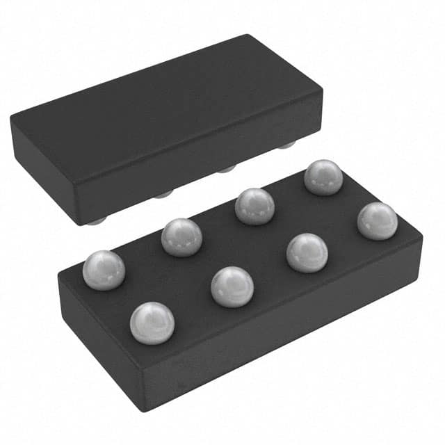
- Package: 8-Pin VSSOP (Very Small Outline Package)
- Essence: This IC is designed to provide non-inverting buffer/driver functionality with 3-state output capability.
- Packaging/Quantity: Available in tape and reel packaging, with a quantity of 2500 units per reel.
Specifications
- Supply Voltage Range: 1.65V to 5.5V
- Input Voltage Range: 0V to VCC
- Output Voltage Range: 0V to VCC
- Operating Temperature Range: -40°C to +85°C
- Propagation Delay: 4.3ns (typical) at 3.3V supply voltage
- Output Drive Capability: ±24mA at 3.3V supply voltage
Detailed Pin Configuration
The SN74LVC2G241YEPR has the following pin configuration:
___________
   A1 |           | VCC
   A2 |           | B1
  GND |           | B2
   OE |           | Y1
   Y2 |           | GND
       -----------
Functional Features
- Dual non-inverting buffer/driver with 3-state output capability.
- Low power consumption.
- High-speed operation.
- Supports mixed-mode signal operation on all ports.
- Schmitt-trigger input allows for slow input transition and noise rejection.
Advantages and Disadvantages
Advantages
- Compact package size enables space-saving designs.
- Wide supply voltage range allows for compatibility with various systems.
- 3-state output capability provides flexibility in bus-oriented applications.
- Low power consumption helps to conserve energy.
Disadvantages
- Limited output drive capability compared to some other ICs in the same category.
- Propagation delay may be a concern in high-speed applications.
Working Principles
The SN74LVC2G241YEPR operates as a non-inverting buffer/driver. It takes input signals from pins A1 and A2, and provides amplified and non-inverted output signals at pins Y1 and Y2. The output can be enabled or disabled using the OE (Output Enable) pin. When the OE pin is low, the outputs are in the high-impedance state, allowing multiple devices to share the same bus without interference.
Detailed Application Field Plans
The SN74LVC2G241YEPR is commonly used in various digital systems and applications, including:
- Microcontrollers and microprocessors
- Communication systems
- Data storage devices
- Industrial automation
- Automotive electronics
- Consumer electronics
Detailed and Complete Alternative Models
- SN74LVC2G07: Dual Buffer/Driver with Open-Drain Output
- SN74LVC2G17: Dual Schmitt-Trigger Buffer/Driver
- SN74LVC2G34: Dual Buffer/Driver with 3-State Output
These alternative models offer similar functionality but may have different characteristics or package options.
In conclusion, the SN74LVC2G241YEPR is a versatile integrated circuit that provides non-inverting buffer/driver functionality with 3-state output capability. Its compact size, wide supply voltage range, and low power consumption make it suitable for various digital applications. However, designers should consider its limited output drive capability and propagation delay when selecting this IC for high-speed applications.
Enumere 10 preguntas y respuestas comunes relacionadas con la aplicación de SN74LVC2G241YEPR en soluciones técnicas
Sure! Here are 10 common questions and answers related to the application of SN74LVC2G241YEPR:
Q: What is SN74LVC2G241YEPR? A: SN74LVC2G241YEPR is a dual buffer/driver IC (integrated circuit) that can be used for signal amplification, buffering, and level shifting in various technical solutions.
Q: What is the voltage range supported by SN74LVC2G241YEPR? A: SN74LVC2G241YEPR supports a voltage range of 1.65V to 5.5V, making it compatible with a wide range of devices and systems.
Q: Can SN74LVC2G241YEPR be used for bidirectional communication? A: Yes, SN74LVC2G241YEPR supports bidirectional communication, allowing signals to be transmitted and received on the same pin.
Q: What is the maximum output current of SN74LVC2G241YEPR? A: SN74LVC2G241YEPR can provide a maximum output current of 24mA, which is sufficient for driving standard logic levels.
Q: Is SN74LVC2G241YEPR suitable for high-speed applications? A: Yes, SN74LVC2G241YEPR is designed for high-speed operation and can support data rates up to several hundred megahertz (MHz).
Q: Can SN74LVC2G241YEPR tolerate overvoltage or ESD events? A: SN74LVC2G241YEPR has built-in protection features to withstand overvoltage and electrostatic discharge (ESD) events, ensuring robustness in real-world scenarios.
Q: How many input and output pins does SN74LVC2G241YEPR have? A: SN74LVC2G241YEPR has two input pins and two output pins, making it suitable for applications requiring dual buffering or driving.
Q: Can SN74LVC2G241YEPR be used in battery-powered devices? A: Yes, SN74LVC2G241YEPR is designed to operate with low power consumption, making it suitable for battery-powered devices where energy efficiency is crucial.
Q: Is SN74LVC2G241YEPR compatible with other logic families? A: SN74LVC2G241YEPR is compatible with a wide range of logic families, including TTL, CMOS, and LVTTL, allowing seamless integration into existing systems.
Q: What package options are available for SN74LVC2G241YEPR? A: SN74LVC2G241YEPR is available in various package options, such as SOT-23, VSSOP, and DSBGA, providing flexibility for different PCB layouts and space constraints.
Please note that the answers provided here are general and may vary depending on specific application requirements. It's always recommended to refer to the datasheet and consult with technical experts for accurate information.