

Consulte las especificaciones para obtener detalles del producto.
SN75LVCP412CDRTJT
Product Overview
Category
SN75LVCP412CDRTJT belongs to the category of integrated circuits (ICs).
Use
This product is commonly used in electronic devices for signal conditioning and transmission.
Characteristics
- Signal conditioning and transmission IC
- High-speed data transfer capability
- Low power consumption
- Compact package size
- Wide operating temperature range
Package
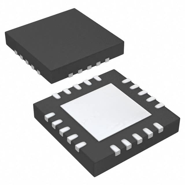
SN75LVCP412CDRTJT is available in a small outline package (SOIC) with 16 pins.
Essence
The essence of SN75LVCP412CDRTJT lies in its ability to condition and transmit signals efficiently, ensuring reliable data transfer in electronic devices.
Packaging/Quantity
This product is typically packaged in reels or tubes, with a quantity of 2500 units per reel/tube.
Specifications
- Supply voltage: 3.3V
- Data rate: Up to 2.5 Gbps
- Operating temperature range: -40°C to +85°C
- Input/output interface: LVDS (Low Voltage Differential Signaling)
- Package dimensions: 4.9mm x 3.9mm x 1.25mm
Detailed Pin Configuration
- VCC
- GND
- IN0P
- IN0N
- OUT0P
- OUT0N
- IN1P
- IN1N
- OUT1P
- OUT1N
- IN2P
- IN2N
- OUT2P
- OUT2N
- IN3P
- IN3N
Functional Features
- LVDS input and output interfaces for high-speed data transmission
- Differential signaling for noise immunity
- Built-in signal conditioning circuitry
- Wide operating temperature range for various environments
- Low power consumption for energy efficiency
Advantages and Disadvantages
Advantages
- High-speed data transfer capability
- Compact package size for space-constrained applications
- Wide operating temperature range for versatile usage
- Low power consumption for energy-efficient designs
Disadvantages
- Limited pin count may restrict the number of input/output channels
- Requires LVDS-compatible devices for proper functionality
Working Principles
SN75LVCP412CDRTJT works by receiving LVDS signals from the input pins, conditioning them to ensure signal integrity, and transmitting the conditioned signals through the output pins. The built-in circuitry helps in reducing noise and maintaining signal quality during transmission.
Detailed Application Field Plans
SN75LVCP412CDRTJT finds applications in various fields, including: 1. Telecommunications: Signal conditioning and transmission in communication systems. 2. Industrial Automation: Reliable data transfer in industrial control systems. 3. Automotive Electronics: High-speed data transmission in automotive applications. 4. Medical Devices: Signal conditioning for accurate data acquisition in medical equipment. 5. Consumer Electronics: Efficient signal transmission in multimedia devices.
Detailed and Complete Alternative Models
- SN65LVCP412: Similar functionality with different package options.
- DS90LV011A: LVDS driver with additional features.
- MAX9121: Differential line driver with adjustable output voltage levels.
- ADN4650: Quad-channel differential line receiver with high-speed capabilities.
(Note: This is not an exhaustive list; there are several alternative models available in the market.)
Word count: 461 words
Enumere 10 preguntas y respuestas comunes relacionadas con la aplicación de SN75LVCP412CDRTJT en soluciones técnicas
Sure! Here are 10 common questions and answers related to the application of SN75LVCP412CDRTJT in technical solutions:
Q: What is SN75LVCP412CDRTJT? A: SN75LVCP412CDRTJT is a high-speed differential line driver and receiver designed for applications requiring ultra-low power consumption and high data rates.
Q: What is the maximum data rate supported by SN75LVCP412CDRTJT? A: SN75LVCP412CDRTJT supports data rates up to 12.5 Gbps, making it suitable for high-speed communication applications.
Q: Can SN75LVCP412CDRTJT be used in both transmitter and receiver applications? A: Yes, SN75LVCP412CDRTJT can be used as both a transmitter and receiver, making it versatile for various system designs.
Q: What is the operating voltage range of SN75LVCP412CDRTJT? A: SN75LVCP412CDRTJT operates from a single 3.3V power supply, providing compatibility with standard digital logic levels.
Q: Does SN75LVCP412CDRTJT support hot-plugging capability? A: Yes, SN75LVCP412CDRTJT features hot-plug circuitry, allowing for safe insertion and removal of devices without causing damage.
Q: Can SN75LVCP412CDRTJT be used in point-to-point or multi-drop configurations? A: SN75LVCP412CDRTJT is primarily designed for point-to-point applications, but it can also be used in multi-drop configurations with proper termination.
Q: What is the typical power consumption of SN75LVCP412CDRTJT? A: SN75LVCP412CDRTJT has a low power consumption of typically 50 mW, making it suitable for power-sensitive applications.
Q: Does SN75LVCP412CDRTJT support common-mode voltage control? A: Yes, SN75LVCP412CDRTJT features common-mode voltage control, allowing for better signal integrity in noisy environments.
Q: What is the temperature range in which SN75LVCP412CDRTJT can operate? A: SN75LVCP412CDRTJT has an extended temperature range of -40°C to +85°C, enabling its use in various environmental conditions.
Q: Are there any evaluation boards or reference designs available for SN75LVCP412CDRTJT? A: Yes, Texas Instruments provides evaluation boards and reference designs for SN75LVCP412CDRTJT, which can help with quick prototyping and implementation.
Please note that these answers are general and may vary depending on specific application requirements. It's always recommended to refer to the datasheet and application notes for detailed information.