

Consulte las especificaciones para obtener detalles del producto.
TLC5540CNSR
Product Overview
Category
The TLC5540CNSR belongs to the category of analog-to-digital converters (ADCs).
Use
It is primarily used for converting analog signals into digital data.
Characteristics
- High resolution: The TLC5540CNSR offers a resolution of 12 bits, allowing for precise conversion of analog signals.
- Low power consumption: This ADC operates at low power, making it suitable for battery-powered devices.
- Fast conversion speed: With a maximum conversion rate of 200 kilosamples per second (ksps), it can quickly convert analog signals into digital form.
- Wide input voltage range: The TLC5540CNSR can handle input voltages ranging from 0 to Vref, providing flexibility in various applications.
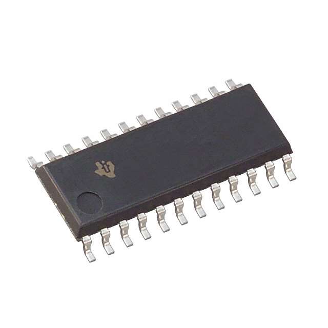
Package and Quantity
The TLC5540CNSR comes in a small outline integrated circuit (SOIC) package. It is available in tape and reel packaging, with a quantity of 2500 units per reel.
Specifications
- Resolution: 12 bits
- Conversion Rate: Up to 200 ksps
- Input Voltage Range: 0 to Vref
- Power Supply: 5V
- Operating Temperature Range: -40°C to +85°C
Pin Configuration
The TLC5540CNSR has a total of 28 pins. Here is the detailed pin configuration:
- VREFH: Reference voltage high
- VREFL: Reference voltage low
- AGND: Analog ground
- REFOUT: Reference output
- INCOM: Common-mode input
- VIN: Analog input
- VREFP: Positive reference voltage
- VDD: Power supply
- D11-D0: Digital outputs
- CS: Chip select
- RD: Read
- WR: Write
- ALE: Address latch enable
- OE: Output enable
- CLK: Clock
Functional Features
- Successive Approximation Register (SAR) architecture: The TLC5540CNSR utilizes SAR architecture for accurate and efficient analog-to-digital conversion.
- Internal voltage reference: It incorporates an internal voltage reference, eliminating the need for an external reference source.
- Serial interface: The ADC communicates with the microcontroller or other devices through a serial interface, simplifying integration into various systems.
- Programmable gain amplifier: The TLC5540CNSR includes a programmable gain amplifier that allows for amplification of weak input signals.
Advantages and Disadvantages
Advantages
- High resolution enables precise measurement and control applications.
- Low power consumption makes it suitable for battery-powered devices.
- Fast conversion speed allows for real-time data acquisition.
- Wide input voltage range provides flexibility in various applications.
Disadvantages
- Limited to 12-bit resolution, which may not be sufficient for certain high-precision applications.
- Requires an external clock signal for operation.
Working Principles
The TLC5540CNSR operates based on the successive approximation method. It samples the analog input voltage and compares it to a digital representation obtained from the internal digital-to-analog converter (DAC). By iteratively adjusting the DAC output, the ADC converges towards the input voltage value, resulting in a digital representation of the analog signal.
Detailed Application Field Plans
The TLC5540CNSR finds applications in various fields, including:
- Industrial automation: It can be used for monitoring and controlling analog signals in industrial processes.
- Medical equipment: The ADC is suitable for medical devices that require accurate measurement of physiological signals.
- Data acquisition systems: It is commonly employed in data acquisition systems for converting analog sensor outputs into digital data.
- Instrumentation: The TLC5540CNSR is utilized in precision instruments for accurate measurement and control.
Alternative Models
Here are some alternative models that offer similar functionality:
- ADC0804: 8-bit analog-to-digital converter with a lower resolution but simpler interface.
- ADS124S08: 24-bit ADC with higher resolution and integrated features for precision applications.
- MCP3208: 12-bit ADC with SPI interface, suitable for low-cost applications.
These alternative models provide options based on specific requirements and constraints.
In conclusion, the TLC5540CNSR is a high-resolution analog-to-digital converter with low power consumption and fast conversion speed. It finds applications in various fields, including industrial automation, medical equipment, data acquisition systems, and instrumentation. While it has certain limitations, alternative models are available to cater to different needs.
Enumere 10 preguntas y respuestas comunes relacionadas con la aplicación de TLC5540CNSR en soluciones técnicas
Sure! Here are 10 common questions and answers related to the application of TLC5540CNSR in technical solutions:
Q: What is TLC5540CNSR? A: TLC5540CNSR is a 12-bit analog-to-digital converter (ADC) integrated circuit commonly used in various technical applications.
Q: What is the operating voltage range of TLC5540CNSR? A: The operating voltage range of TLC5540CNSR is typically between 4.5V and 6V.
Q: What is the maximum sampling rate of TLC5540CNSR? A: The maximum sampling rate of TLC5540CNSR is 40 kilosamples per second (ksps).
Q: How many analog input channels does TLC5540CNSR have? A: TLC5540CNSR has a total of 11 analog input channels.
Q: What is the resolution of TLC5540CNSR? A: TLC5540CNSR has a resolution of 12 bits, which means it can provide 4096 discrete digital output values.
Q: Can TLC5540CNSR operate in both single-ended and differential mode? A: Yes, TLC5540CNSR can be configured to operate in both single-ended and differential mode depending on the application requirements.
Q: What is the typical power consumption of TLC5540CNSR? A: The typical power consumption of TLC5540CNSR is around 15 milliwatts (mW).
Q: Does TLC5540CNSR have an internal reference voltage? A: No, TLC5540CNSR does not have an internal reference voltage. An external reference voltage needs to be provided for accurate conversions.
Q: What is the output interface of TLC5540CNSR? A: TLC5540CNSR provides a parallel digital output interface, making it compatible with various microcontrollers and digital systems.
Q: Can TLC5540CNSR operate in harsh environments? A: TLC5540CNSR is not specifically designed for harsh environments. It is recommended to use appropriate protective measures if operating in such conditions.
Please note that these answers are general and may vary depending on the specific datasheet and application requirements.