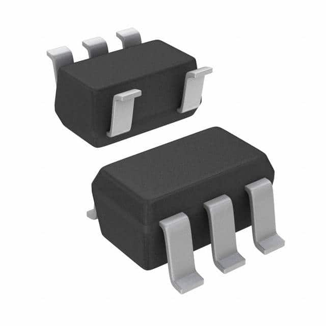
Consulte las especificaciones para obtener detalles del producto.

TLV1391CDBVTG4
Product Overview
- Category: Integrated Circuit (IC)
- Use: Voltage Comparator
- Characteristics: Low-power, Rail-to-Rail Input/Output, Push-Pull Output, Small Package Size
- Package: SOT-23-6
- Essence: TLV1391CDBVTG4 is a voltage comparator IC designed for low-power applications. It provides rail-to-rail input and output capabilities with a push-pull output stage. The small package size makes it suitable for space-constrained designs.
- Packaging/Quantity: Available in tape and reel packaging, with 3000 units per reel.
Specifications
- Supply Voltage Range: 2 V to 36 V
- Input Offset Voltage: ±1 mV (maximum)
- Input Bias Current: ±5 nA (maximum)
- Response Time: 3 µs (typical)
- Operating Temperature Range: -40°C to +125°C
- Input Common Mode Voltage Range: -0.1 V to VCC+0.1 V
Pin Configuration
The TLV1391CDBVTG4 IC has the following pin configuration:
____
   IN-|    |
   IN+|    |
   GND|    |
   OUT|    |
   VCC|    |
   NC-|____|
Functional Features
- Low-power consumption: The TLV1391CDBVTG4 operates at low power levels, making it suitable for battery-powered devices.
- Rail-to-rail input/output: It can accept input signals that span the entire supply voltage range and provide output signals that approach the supply rails.
- Push-pull output: The IC features a push-pull output stage, allowing it to drive both high and low loads efficiently.
- Small package size: The SOT-23-6 package is compact, enabling space-saving designs.
Advantages and Disadvantages
Advantages: - Low-power consumption extends battery life in portable applications. - Rail-to-rail input/output allows for versatile signal handling. - Push-pull output stage ensures efficient driving of loads. - Small package size enables compact designs.
Disadvantages: - Limited number of pins may restrict the complexity of circuits that can be implemented. - Not suitable for high-voltage applications due to the maximum supply voltage limitation.
Working Principles
The TLV1391CDBVTG4 is a voltage comparator that compares the voltage at its non-inverting input (IN+) with the voltage at its inverting input (IN-). It amplifies the voltage difference between the inputs and produces a digital output signal based on the comparison result. The rail-to-rail input/output capability allows it to operate with signals that span the entire supply voltage range.
Detailed Application Field Plans
The TLV1391CDBVTG4 is commonly used in various applications, including but not limited to:
- Battery-powered devices: Due to its low-power consumption, the IC is suitable for use in portable electronics such as smartphones, tablets, and wearable devices.
- Sensor interfaces: The comparator can be used to interface with sensors that provide analog voltage outputs, allowing for precise threshold detection.
- Signal conditioning: It can be employed in signal conditioning circuits to amplify or attenuate signals before further processing.
- Motor control: The push-pull output stage makes it suitable for motor control applications, where it can drive transistors or other devices to control motor speed or direction.
Detailed and Complete Alternative Models
Some alternative models to TLV1391CDBVTG4 include:
- LM339: A quad voltage comparator with similar characteristics and package options.
- MAX9025: A low-power, single-supply voltage comparator with rail-to-rail inputs and push-pull outputs.
- LT1716: A micropower, dual voltage comparator with a wide supply voltage range and small package size.
These alternative models offer similar functionality and can be considered based on specific application requirements.
Word count: 410 words
Enumere 10 preguntas y respuestas comunes relacionadas con la aplicación de TLV1391CDBVTG4 en soluciones técnicas
Sure! Here are 10 common questions and answers related to the application of TLV1391CDBVTG4:
Q1: What is TLV1391CDBVTG4? A1: TLV1391CDBVTG4 is a precision voltage comparator with an open-drain output. It is commonly used in various technical solutions.
Q2: What is the operating voltage range for TLV1391CDBVTG4? A2: The operating voltage range for TLV1391CDBVTG4 is typically between 2.7V and 36V.
Q3: What is the typical input offset voltage of TLV1391CDBVTG4? A3: The typical input offset voltage of TLV1391CDBVTG4 is around 1mV.
Q4: Can TLV1391CDBVTG4 operate in high-temperature environments? A4: Yes, TLV1391CDBVTG4 has a wide temperature range and can operate in high-temperature environments up to 125°C.
Q5: What is the maximum supply current required by TLV1391CDBVTG4? A5: The maximum supply current required by TLV1391CDBVTG4 is typically 1.6mA.
Q6: Is TLV1391CDBVTG4 suitable for battery-powered applications? A6: Yes, TLV1391CDBVTG4 is suitable for battery-powered applications due to its low supply current and wide operating voltage range.
Q7: Can TLV1391CDBVTG4 be used as a level shifter? A7: Yes, TLV1391CDBVTG4 can be used as a level shifter to convert signals between different voltage levels.
Q8: What is the output voltage range of TLV1391CDBVTG4? A8: The output voltage range of TLV1391CDBVTG4 is typically between ground and the supply voltage.
Q9: Does TLV1391CDBVTG4 have built-in hysteresis? A9: Yes, TLV1391CDBVTG4 has built-in hysteresis to provide noise immunity and prevent output oscillation near the threshold voltage.
Q10: Can TLV1391CDBVTG4 be used in automotive applications? A10: Yes, TLV1391CDBVTG4 is suitable for automotive applications as it meets the necessary standards and can operate in a wide temperature range.
Please note that these answers are general and may vary depending on specific datasheet specifications and application requirements.

