

Consulte las especificaciones para obtener detalles del producto.
XC6108C19BGR-G
Product Overview
Category
XC6108C19BGR-G belongs to the category of electronic components.
Use
It is commonly used in electronic circuits for voltage regulation and power management purposes.
Characteristics
- Voltage regulation capabilities
- Compact size
- Low power consumption
- High efficiency
Package
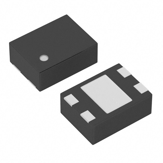
XC6108C19BGR-G is available in a small surface-mount package, which makes it suitable for integration into various electronic devices.
Essence
The essence of XC6108C19BGR-G lies in its ability to regulate voltage levels within electronic circuits, ensuring stable and reliable operation.
Packaging/Quantity
This product is typically packaged in reels or tubes, with each reel or tube containing a specific quantity of XC6108C19BGR-G units. The exact packaging and quantity may vary depending on the manufacturer.
Specifications
- Input Voltage Range: 2.5V - 6.0V
- Output Voltage: 1.9V
- Maximum Output Current: 100mA
- Dropout Voltage: 200mV (typical)
- Quiescent Current: 30μA (typical)
- Operating Temperature Range: -40°C to +85°C
Detailed Pin Configuration
XC6108C19BGR-G has the following pin configuration:
- VIN (Input Voltage)
- GND (Ground)
- VOUT (Output Voltage)
Functional Features
- Voltage Regulation: XC6108C19BGR-G ensures a stable output voltage of 1.9V regardless of input voltage fluctuations.
- Overcurrent Protection: It incorporates overcurrent protection to safeguard the circuit from excessive current flow.
- Low Power Consumption: The device itself consumes minimal power, contributing to energy efficiency in electronic systems.
Advantages and Disadvantages
Advantages
- Compact size allows for easy integration into space-constrained designs.
- High efficiency results in minimal power loss during voltage regulation.
- Wide input voltage range provides flexibility in various applications.
Disadvantages
- Limited output current capacity may not be suitable for high-power applications.
- Dropout voltage of 200mV may affect the overall efficiency in certain scenarios.
Working Principles
XC6108C19BGR-G utilizes a voltage reference and feedback mechanism to maintain a constant output voltage. It compares the output voltage with a reference voltage and adjusts the internal circuitry accordingly to regulate the output voltage at the desired level.
Detailed Application Field Plans
XC6108C19BGR-G finds application in various electronic devices, including but not limited to: - Mobile phones - Portable media players - Wearable devices - IoT devices - Battery-powered systems
Detailed and Complete Alternative Models
Some alternative models that provide similar functionality to XC6108C19BGR-G are: - XC6206P192MR-G - LM1117IMPX-1.9/NOPB - MCP1700T-1902E/TT
Enumere 10 preguntas y respuestas comunes relacionadas con la aplicación de XC6108C19BGR-G en soluciones técnicas
Sure! Here are 10 common questions and answers related to the application of XC6108C19BGR-G in technical solutions:
Q: What is XC6108C19BGR-G? A: XC6108C19BGR-G is a voltage detector IC (integrated circuit) that monitors the power supply voltage and provides a reset signal when the voltage drops below a certain threshold.
Q: What is the operating voltage range of XC6108C19BGR-G? A: The operating voltage range of XC6108C19BGR-G is typically between 0.9V and 6.0V.
Q: How does XC6108C19BGR-G help in technical solutions? A: XC6108C19BGR-G helps in technical solutions by ensuring proper system operation and preventing data corruption or malfunctioning caused by low voltage conditions.
Q: Can XC6108C19BGR-G be used in battery-powered applications? A: Yes, XC6108C19BGR-G can be used in battery-powered applications as it has a low quiescent current consumption of typically 1.0µA.
Q: What is the reset output type of XC6108C19BGR-G? A: XC6108C19BGR-G provides an active-low reset output.
Q: What is the typical reset threshold voltage of XC6108C19BGR-G? A: The typical reset threshold voltage of XC6108C19BGR-G is 1.9V.
Q: Does XC6108C19BGR-G have any built-in delay time for the reset signal? A: Yes, XC6108C19BGR-G has a built-in delay time of typically 200ms to ensure stable power supply before releasing the reset signal.
Q: Can XC6108C19BGR-G be used in automotive applications? A: Yes, XC6108C19BGR-G is suitable for automotive applications as it meets the AEC-Q100 Grade 2 qualification standards.
Q: Does XC6108C19BGR-G have any additional features for fault detection? A: No, XC6108C19BGR-G is a basic voltage detector IC and does not have additional fault detection features.
Q: What package type is XC6108C19BGR-G available in? A: XC6108C19BGR-G is available in a SOT-25 package, which is a small surface-mount package with 5 pins.
Please note that the answers provided here are general and may vary depending on the specific datasheet and manufacturer's specifications of XC6108C19BGR-G.