

Consulte las especificaciones para obtener detalles del producto.
XC61CC3202MR-G
Product Overview
Category
XC61CC3202MR-G belongs to the category of electronic components.
Use
It is commonly used in various electronic devices and circuits for voltage regulation and power management purposes.
Characteristics
- Low dropout voltage
- High output voltage accuracy
- Low quiescent current
- Thermal shutdown protection
- Short circuit current limit
Package
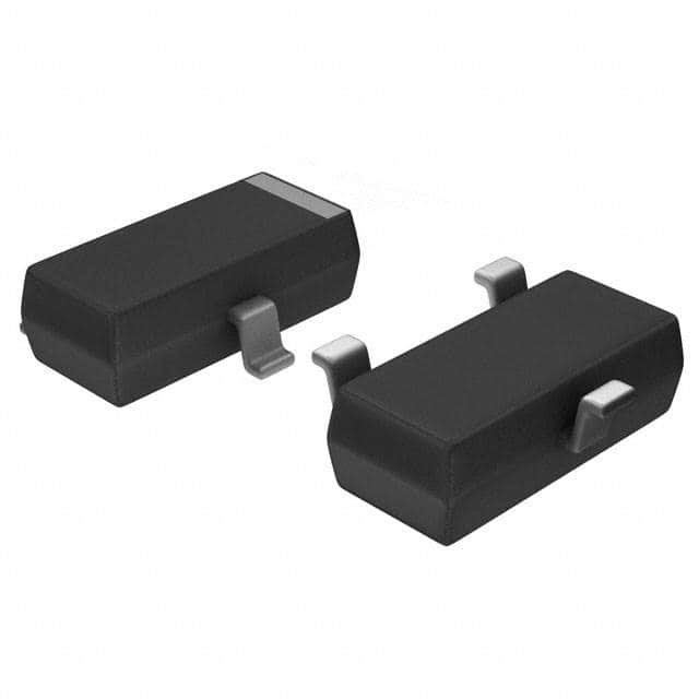
XC61CC3202MR-G is available in a small surface mount package, typically SOT-23-3.
Essence
The essence of XC61CC3202MR-G lies in its ability to provide stable and regulated voltage output for electronic systems.
Packaging/Quantity
XC61CC3202MR-G is usually packaged in reels or tape and reel packaging, with a quantity of 3000 units per reel.
Specifications
- Input Voltage Range: 2.5V to 6.0V
- Output Voltage Range: 1.2V to 5.0V
- Dropout Voltage: 200mV (typical)
- Quiescent Current: 30μA (typical)
- Output Current: 100mA (maximum)
Detailed Pin Configuration
XC61CC3202MR-G has three pins:
- VIN: Input voltage pin
- GND: Ground pin
- VOUT: Output voltage pin
Functional Features
- Low dropout voltage ensures efficient power conversion.
- High output voltage accuracy provides precise voltage regulation.
- Low quiescent current minimizes power consumption.
- Thermal shutdown protection prevents overheating.
- Short circuit current limit protects the device from damage during fault conditions.
Advantages and Disadvantages
Advantages
- Compact size and surface mount package make it suitable for space-constrained applications.
- Wide input voltage range allows compatibility with various power sources.
- High output voltage accuracy ensures reliable performance.
- Low quiescent current extends battery life in portable devices.
Disadvantages
- Limited output current may not be suitable for high-power applications.
- Dropout voltage may cause a slight voltage drop across the device.
Working Principles
XC61CC3202MR-G is a linear voltage regulator that uses a pass transistor to regulate the output voltage. It compares the reference voltage with the feedback voltage and adjusts the pass transistor accordingly to maintain a stable output voltage.
Detailed Application Field Plans
XC61CC3202MR-G can be used in various electronic devices and circuits, including but not limited to: - Mobile phones - Portable media players - Digital cameras - Wireless communication devices - Battery-powered systems
Detailed and Complete Alternative Models
Some alternative models to XC61CC3202MR-G are: - XC61CC3202MR-G-ND - XC61CC3202MR-GCT-ND - XC61CC3202MR-GCT-ND-DS
These alternative models offer similar functionality and characteristics, providing options for different application requirements.
Word count: 431 words
Enumere 10 preguntas y respuestas comunes relacionadas con la aplicación de XC61CC3202MR-G en soluciones técnicas
Sure! Here are 10 common questions and answers related to the application of XC61CC3202MR-G in technical solutions:
Question: What is XC61CC3202MR-G?
- Answer: XC61CC3202MR-G is a voltage detector IC manufactured by Torex Semiconductor. It is commonly used for power supply monitoring and reset functions in various electronic devices.Question: What is the operating voltage range of XC61CC3202MR-G?
- Answer: The operating voltage range of XC61CC3202MR-G is from 0.9V to 6.0V.Question: What is the output type of XC61CC3202MR-G?
- Answer: XC61CC3202MR-G has an open-drain output type, which means it can be connected to other devices with a pull-up resistor to achieve different logic levels.Question: What is the typical quiescent current consumption of XC61CC3202MR-G?
- Answer: The typical quiescent current consumption of XC61CC3202MR-G is around 1.0µA, making it suitable for low-power applications.Question: How does XC61CC3202MR-G detect voltage levels?
- Answer: XC61CC3202MR-G uses a built-in voltage reference and comparator to detect voltage levels. When the input voltage exceeds the detection threshold, the output goes low.Question: Can XC61CC3202MR-G be used for overvoltage protection?
- Answer: No, XC61CC3202MR-G is not designed for overvoltage protection. It is primarily used for power supply monitoring and reset functions.Question: What is the maximum voltage that XC61CC3202MR-G can tolerate?
- Answer: The maximum voltage that XC61CC3202MR-G can tolerate is 6.5V. Exceeding this voltage may damage the IC.Question: Can XC61CC3202MR-G be used in automotive applications?
- Answer: Yes, XC61CC3202MR-G is AEC-Q100 qualified and suitable for automotive applications where power supply monitoring and reset functions are required.Question: Does XC61CC3202MR-G have any built-in delay time?
- Answer: No, XC61CC3202MR-G does not have a built-in delay time. If a delay is required, an external capacitor can be connected to the CDET pin.Question: What is the package type of XC61CC3202MR-G?
- Answer: XC61CC3202MR-G is available in a SOT-23-3 package, which is a small surface-mount package commonly used in electronic devices.
Please note that these answers are based on general information about XC61CC3202MR-G, and it's always recommended to refer to the datasheet and consult with the manufacturer for specific application requirements.