

Consulte las especificaciones para obtener detalles del producto.
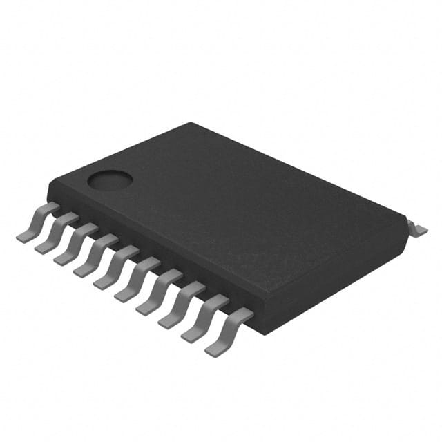
74LCX574FT
Basic Information Overview
- Category: Integrated Circuit (IC)
- Use: Flip-Flop
- Characteristics: Low-voltage, CMOS technology
- Package: TSSOP (Thin Shrink Small Outline Package)
- Essence: Octal D-type flip-flop with 3-state outputs
- Packaging/Quantity: Tape and Reel, 2500 units per reel
Specifications
- Supply Voltage Range: 2.0V to 3.6V
- High-Level Input Voltage: 2.0V to VCC + 0.5V
- Low-Level Input Voltage: -0.5V to 0.8V
- High-Level Output Voltage: VCC - 0.5V
- Low-Level Output Voltage: 0.5V
- Maximum Input Current: ±10mA
- Maximum Output Current: ±24mA
- Operating Temperature Range: -40°C to +85°C
Detailed Pin Configuration
The 74LCX574FT has a total of 20 pins, which are arranged as follows:
- GND - Ground
- D0 - Data input for flip-flop 0
- D1 - Data input for flip-flop 1
- D2 - Data input for flip-flop 2
- D3 - Data input for flip-flop 3
- D4 - Data input for flip-flop 4
- D5 - Data input for flip-flop 5
- D6 - Data input for flip-flop 6
- D7 - Data input for flip-flop 7
- Q7 - Output for flip-flop 7
- Q6 - Output for flip-flop 6
- Q5 - Output for flip-flop 5
- Q4 - Output for flip-flop 4
- Q3 - Output for flip-flop 3
- Q2 - Output for flip-flop 2
- Q1 - Output for flip-flop 1
- Q0 - Output for flip-flop 0
- OE - Output Enable
- CP - Clock Pulse input
- VCC - Power supply
Functional Features
- Octal D-type flip-flop with 3-state outputs
- Low-voltage operation, suitable for battery-powered devices
- CMOS technology ensures low power consumption and high noise immunity
- 3-state outputs allow multiple devices to share a common bus
Advantages and Disadvantages
Advantages: - Low-voltage operation extends battery life in portable applications - CMOS technology provides high noise immunity - 3-state outputs enable efficient bus sharing
Disadvantages: - Limited operating temperature range (-40°C to +85°C) - Requires external clock pulse for proper operation
Working Principles
The 74LCX574FT is an octal D-type flip-flop with 3-state outputs. It stores data on its inputs (D0-D7) based on the rising edge of the clock pulse (CP). The stored data is then available on the corresponding outputs (Q0-Q7). The Output Enable (OE) pin controls whether the outputs are active or in a high-impedance state.
Detailed Application Field Plans
The 74LCX574FT is commonly used in various digital systems where the storage and retrieval of data is required. Some application fields include: - Microcontrollers - Data communication systems - Memory modules - Industrial automation - Automotive electronics
Detailed and Complete Alternative Models
Some alternative models that offer similar functionality to the 74LCX574FT are: - 74HC574: High-speed CMOS version - SN74LV574A: Low-voltage TTL version - CD4013B: Dual D-type flip-flop with 3-state outputs
Note: The above alternatives may have different pin configurations and specifications. It is important to refer to their respective datasheets for detailed information.
Word count: 416 words
Enumere 10 preguntas y respuestas comunes relacionadas con la aplicación de 74LCX574FT en soluciones técnicas
Sure! Here are 10 common questions and answers related to the application of 74LCX574FT in technical solutions:
Q: What is the 74LCX574FT? A: The 74LCX574FT is a flip-flop IC (integrated circuit) that consists of eight D-type flip-flops with tri-state outputs.
Q: What is the purpose of using the 74LCX574FT in a technical solution? A: The 74LCX574FT is commonly used for data storage, synchronization, and signal buffering in digital circuits.
Q: What is the maximum operating voltage for the 74LCX574FT? A: The 74LCX574FT has a maximum operating voltage of 3.6V.
Q: Can the 74LCX574FT be used with both TTL and CMOS logic levels? A: Yes, the 74LCX574FT is compatible with both TTL and CMOS logic levels.
Q: How many inputs and outputs does the 74LCX574FT have? A: The 74LCX574FT has eight inputs and eight outputs.
Q: What is the function of the tri-state outputs in the 74LCX574FT? A: The tri-state outputs allow the outputs to be disabled or put into a high-impedance state when not needed, which helps in bus sharing applications.
Q: What is the typical propagation delay of the 74LCX574FT? A: The typical propagation delay of the 74LCX574FT is around 3.8 ns.
Q: Can the 74LCX574FT be cascaded to increase the number of flip-flops? A: Yes, multiple 74LCX574FT ICs can be cascaded to increase the number of flip-flops in a circuit.
Q: Does the 74LCX574FT have any built-in clock or enable signals? A: No, the 74LCX574FT does not have any built-in clock or enable signals. External clock and enable signals need to be provided.
Q: What is the power supply voltage range for the 74LCX574FT? A: The power supply voltage range for the 74LCX574FT is typically between 2.0V and 3.6V.
Please note that these answers are general and may vary depending on the specific datasheet and manufacturer's specifications for the 74LCX574FT.