

Consulte las especificaciones para obtener detalles del producto.
TC7WBD125AFKT5LF
Basic Information Overview
- Category: Integrated Circuit (IC)
- Use: Logic Gate
- Characteristics: High-speed, Low-power consumption
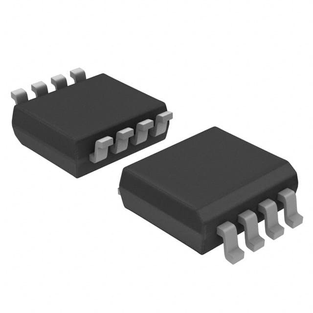
- Package: SOT-353
- Essence: Dual Buffer/Driver
- Packaging/Quantity: Tape and Reel, 3000 pieces per reel
Specifications
- Supply Voltage: 1.65V to 5.5V
- Input Voltage: 0V to VCC
- Output Voltage: 0V to VCC
- Operating Temperature Range: -40°C to +85°C
- Propagation Delay Time: 2.9ns (typical)
- Output Current: ±24mA (maximum)
Detailed Pin Configuration
The TC7WBD125AFKT5LF has a total of 5 pins arranged as follows:
___________
      |           |
   1 -| A         |
   2 -| B         |
   3 -| Y         |
   4 -| GND       |
   5 -| VCC       |
      |___________|
Pin Description: - Pin 1 (A): Input A - Pin 2 (B): Input B - Pin 3 (Y): Output Y - Pin 4 (GND): Ground - Pin 5 (VCC): Power Supply
Functional Features
- Dual buffer/driver with independent control inputs
- High-speed operation suitable for various applications
- Low-power consumption for energy-efficient designs
- Wide operating voltage range for compatibility with different systems
- Output current capability allows driving of external loads
Advantages and Disadvantages
Advantages: - High-speed operation enables efficient data processing - Low-power consumption prolongs battery life in portable devices - Wide operating voltage range ensures compatibility with different systems
Disadvantages: - Limited output current may restrict driving capability for certain applications - SOT-353 package may require careful handling during assembly
Working Principles
The TC7WBD125AFKT5LF is a dual buffer/driver IC that provides independent control inputs for each buffer. It operates by receiving input signals (A and B) and producing corresponding output signals (Y). The device functions as a voltage level translator, allowing seamless communication between different logic families or voltage domains.
Detailed Application Field Plans
The TC7WBD125AFKT5LF can be used in various applications, including but not limited to: 1. Microcontrollers and microprocessors 2. Communication systems 3. Data storage devices 4. Industrial automation 5. Automotive electronics
Detailed and Complete Alternative Models
- SN74LVC2G07: Dual Buffer/Driver, SOT-353 package
- MC74VHC1GT125: Single Buffer/Driver, SOT-353 package
- 74HC244: Octal Buffer/Line Driver, SOIC package
- CD40109B: Quad Buffer/Line Driver, DIP package
- NC7SZ125: Single Buffer/Driver, SC-70 package
These alternative models offer similar functionality and can be considered as substitutes for the TC7WBD125AFKT5LF based on specific requirements and availability.
Word count: 303 words
Enumere 10 preguntas y respuestas comunes relacionadas con la aplicación de TC7WBD125AFKT5LF en soluciones técnicas
Sure! Here are 10 common questions and answers related to the application of TC7WBD125AFKT5LF in technical solutions:
Q: What is TC7WBD125AFKT5LF? A: TC7WBD125AFKT5LF is a specific model of logic gate IC (integrated circuit) used for signal processing and voltage level shifting.
Q: What is the operating voltage range of TC7WBD125AFKT5LF? A: The operating voltage range of TC7WBD125AFKT5LF is typically between 1.65V and 5.5V.
Q: What is the maximum output current of TC7WBD125AFKT5LF? A: The maximum output current of TC7WBD125AFKT5LF is typically around 32mA.
Q: Can TC7WBD125AFKT5LF be used as a level shifter? A: Yes, TC7WBD125AFKT5LF can be used as a level shifter to convert signals between different voltage levels.
Q: What is the input capacitance of TC7WBD125AFKT5LF? A: The input capacitance of TC7WBD125AFKT5LF is typically around 3pF.
Q: Is TC7WBD125AFKT5LF suitable for high-speed applications? A: Yes, TC7WBD125AFKT5LF is designed for high-speed operation and can be used in applications with fast switching requirements.
Q: Can TC7WBD125AFKT5LF be used in both digital and analog circuits? A: No, TC7WBD125AFKT5LF is primarily designed for digital signal processing and is not recommended for use in analog circuits.
Q: What is the typical propagation delay of TC7WBD125AFKT5LF? A: The typical propagation delay of TC7WBD125AFKT5LF is around 3.5ns.
Q: Does TC7WBD125AFKT5LF have built-in ESD protection? A: Yes, TC7WBD125AFKT5LF has built-in ESD (electrostatic discharge) protection to safeguard against static electricity damage.
Q: Can TC7WBD125AFKT5LF be used in battery-powered applications? A: Yes, TC7WBD125AFKT5LF can be used in battery-powered applications as it operates within a wide voltage range and has low power consumption.
Please note that the answers provided here are general and may vary depending on specific datasheet specifications and application requirements.