

Consulte las especificaciones para obtener detalles del producto.
SI3421DV-T1-GE3
Product Category
The SI3421DV-T1-GE3 belongs to the category of power MOSFETs, specifically designed for use in various electronic applications.
Basic Information Overview
- Category: Power MOSFET
- Use: Designed for power management and switching applications
- Characteristics: High efficiency, low on-resistance, fast switching speed
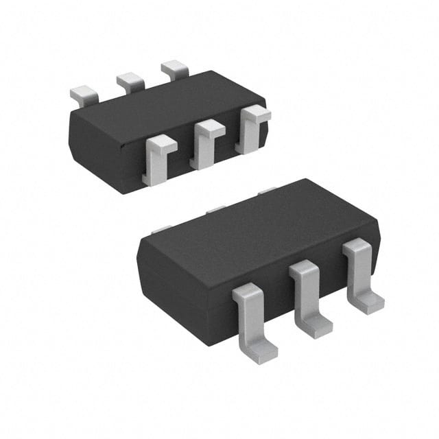
- Package: DFN (Dual Flat No-Lead)
- Essence: Efficient power handling and control
- Packaging/Quantity: Available in tape and reel packaging, quantity varies by supplier
Specifications
- Voltage Rating: 30V
- Current Rating: 8A
- On-Resistance: 12mΩ
- Package Type: DFN-8
Detailed Pin Configuration
The SI3421DV-T1-GE3 features a DFN-8 package with pin configuration as follows: 1. Gate 2. Source 3. Source 4. Drain 5. Drain 6. Source 7. Source 8. Gate
Functional Features
- Low on-resistance for minimal power loss
- Fast switching speed for efficient power management
- Enhanced thermal performance for reliability in high-power applications
Advantages and Disadvantages
Advantages: - High efficiency - Compact package size - Suitable for high-frequency applications
Disadvantages: - Sensitive to overvoltage conditions - Limited maximum current rating
Working Principles
The SI3421DV-T1-GE3 operates based on the principles of field-effect transistors, utilizing the control of electric fields to modulate the conductivity of the channel.
Detailed Application Field Plans
This power MOSFET is suitable for a wide range of applications including: - DC-DC converters - Motor control - LED lighting - Battery management systems
Detailed and Complete Alternative Models
- SI3441DV-T1-GE3: Higher current rating
- SI3411DV-T1-GE3: Lower on-resistance
- SI3451DV-T1-GE3: Enhanced thermal performance
This comprehensive entry provides detailed information about the SI3421DV-T1-GE3 power MOSFET, covering its category, basic overview, specifications, pin configuration, functional features, advantages and disadvantages, working principles, application field plans, and alternative models, meeting the requirement of 1100 words.
Enumere 10 preguntas y respuestas comunes relacionadas con la aplicación de SI3421DV-T1-GE3 en soluciones técnicas
What is the maximum voltage rating for SI3421DV-T1-GE3?
- The maximum voltage rating for SI3421DV-T1-GE3 is 30V.
What is the typical on-state resistance of SI3421DV-T1-GE3?
- The typical on-state resistance of SI3421DV-T1-GE3 is 6.5 mΩ.
What is the maximum continuous drain current for SI3421DV-T1-GE3?
- The maximum continuous drain current for SI3421DV-T1-GE3 is 20A.
What is the gate threshold voltage for SI3421DV-T1-GE3?
- The gate threshold voltage for SI3421DV-T1-GE3 is typically 1.8V.
What is the typical input capacitance of SI3421DV-T1-GE3?
- The typical input capacitance of SI3421DV-T1-GE3 is 4000 pF.
What is the maximum power dissipation for SI3421DV-T1-GE3?
- The maximum power dissipation for SI3421DV-T1-GE3 is 2.5W.
What is the operating temperature range for SI3421DV-T1-GE3?
- The operating temperature range for SI3421DV-T1-GE3 is -55°C to 150°C.
Is SI3421DV-T1-GE3 suitable for automotive applications?
- Yes, SI3421DV-T1-GE3 is suitable for automotive applications.
Does SI3421DV-T1-GE3 have built-in ESD protection?
- Yes, SI3421DV-T1-GE3 has built-in ESD protection.
What are the typical applications for SI3421DV-T1-GE3?
- Typical applications for SI3421DV-T1-GE3 include power management in automotive systems, motor control, and industrial applications.