

Consulte las especificaciones para obtener detalles del producto.
W9825G2JB-75 TR
Product Overview
Category
The W9825G2JB-75 TR belongs to the category of integrated circuits (ICs).
Use
This IC is commonly used in electronic devices for memory storage and retrieval purposes.
Characteristics
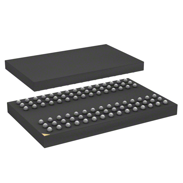
- Package: The W9825G2JB-75 TR is available in a compact surface mount package.
- Essence: It is a high-performance synchronous dynamic random-access memory (SDRAM) chip.
- Packaging/Quantity: This product is typically packaged in reels or trays, with varying quantities depending on customer requirements.
Specifications
The specifications of the W9825G2JB-75 TR are as follows:
- Memory Type: SDRAM
- Capacity: 256 Megabits (32 Megabytes)
- Organization: 4M x 16 bits
- Operating Voltage: 3.3V
- Clock Frequency: 133 MHz
- Access Time: 7.5 ns
- Interface: Parallel
- Refresh Mode: Auto-refresh and self-refresh
- Operating Temperature Range: -40°C to +85°C
Detailed Pin Configuration
The W9825G2JB-75 TR has a specific pin configuration that facilitates its integration into electronic circuits. The detailed pin configuration is as follows:
- VDD
- DQ0
- DQ1
- DQ2
- DQ3
- DQ4
- DQ5
- DQ6
- DQ7
- DQ8
- DQ9
- DQ10
- DQ11
- DQ12
- DQ13
- DQ14
- DQ15
- A0
- A1
- A2
- A3
- A4
- A5
- A6
- A7
- A8
- A9
- A10
- A11
- A12
- A13
- A14
- A15
- /CAS
- /RAS
- /WE
- /CS
- /CKE
- /DQM0
- /DQM1
- /DM
- VSS
Functional Features
The W9825G2JB-75 TR offers the following functional features:
- High-speed data transfer: With a clock frequency of 133 MHz and an access time of 7.5 ns, it enables fast and efficient data transfer.
- Synchronous operation: The IC synchronizes its operations with the system clock, ensuring reliable and accurate data processing.
- Auto-refresh and self-refresh modes: It supports automatic refreshing of stored data, enhancing stability and preventing data loss during power fluctuations.
- Low power consumption: The IC is designed to minimize power consumption, making it suitable for battery-powered devices.
Advantages and Disadvantages
Advantages: - High-performance memory chip - Compact package size - Supports synchronous operation - Automatic and self-refresh modes for data integrity - Low power consumption
Disadvantages: - Limited capacity (256 Megabits) - Parallel interface may require additional circuitry for compatibility with certain systems
Working Principles
The W9825G2JB-75 TR operates based on the principles of synchronous dynamic random-access memory (SDRAM). It stores and retrieves data in a synchronized manner with the system clock. When a read or write operation is initiated, the IC accesses the requested data from the memory array and transfers it to/from the external system.
Detailed Application Field Plans
The W9825G2JB-75 TR finds applications in various electronic devices, including but not limited to: - Personal computers - Laptops and notebooks - Servers - Networking equipment - Consumer electronics (e.g., televisions, gaming consoles) - Mobile devices (e.g., smartphones, tablets)
Detailed and Complete Alternative Models
Some alternative models that offer similar functionality to the W9825G2JB-75 TR include: - W9825G6JB-75 TR - W9825G8JB-75 TR - W9825G16JB-75 TR
These alternative models provide different memory capacities and organizations while maintaining compatibility with the same interface and operating voltage.
In conclusion, the W9825G2JB-75 TR is a high-performance SDRAM chip used for memory storage and retrieval in various electronic devices. Its compact package, synchronous operation, and low power consumption make it a reliable choice for memory-intensive applications. However, its limited capacity and requirement for additional circuitry in certain systems may be considered as disadvantages.
Enumere 10 preguntas y respuestas comunes relacionadas con la aplicación de W9825G2JB-75 TR en soluciones técnicas
Question: What is the W9825G2JB-75 TR?
Answer: The W9825G2JB-75 TR is a specific model of memory chip commonly used in technical solutions.Question: What is the capacity of the W9825G2JB-75 TR?
Answer: The W9825G2JB-75 TR has a capacity of 2 gigabits (Gb).Question: What is the operating voltage range for the W9825G2JB-75 TR?
Answer: The operating voltage range for this memory chip is typically between 2.7V and 3.6V.Question: What is the maximum clock frequency supported by the W9825G2JB-75 TR?
Answer: The W9825G2JB-75 TR supports a maximum clock frequency of 75 MHz.Question: Is the W9825G2JB-75 TR compatible with both commercial and industrial temperature ranges?
Answer: Yes, the W9825G2JB-75 TR is designed to operate within both commercial (0°C to 70°C) and industrial (-40°C to 85°C) temperature ranges.Question: What is the package type of the W9825G2JB-75 TR?
Answer: The W9825G2JB-75 TR comes in a 48-ball FBGA (Fine-Pitch Ball Grid Array) package.Question: Can the W9825G2JB-75 TR be used in automotive applications?
Answer: No, the W9825G2JB-75 TR is not specifically designed or qualified for automotive applications.Question: Does the W9825G2JB-75 TR support multiple banks or channels?
Answer: No, the W9825G2JB-75 TR is a single-bank memory chip.Question: What is the typical access time of the W9825G2JB-75 TR?
Answer: The typical access time for this memory chip is around 70 nanoseconds (ns).Question: Can the W9825G2JB-75 TR be used in both read and write operations?
Answer: Yes, the W9825G2JB-75 TR supports both read and write operations, making it suitable for various technical solutions.