

Consulte las especificaciones para obtener detalles del producto.
XC2C256-6PQ208C
Product Overview
Category
XC2C256-6PQ208C belongs to the category of programmable logic devices (PLDs).
Use
This product is primarily used for digital circuit design and implementation. It provides a flexible and customizable solution for various applications in industries such as telecommunications, automotive, aerospace, and consumer electronics.
Characteristics
- Programmable: XC2C256-6PQ208C can be programmed to perform specific functions based on user requirements.
- High Density: It offers a large number of configurable logic blocks (CLBs) and input/output (I/O) pins, allowing for complex designs.
- Low Power Consumption: The device is designed to operate efficiently with minimal power consumption.
- Fast Operation: XC2C256-6PQ208C provides high-speed performance, enabling quick execution of digital circuits.
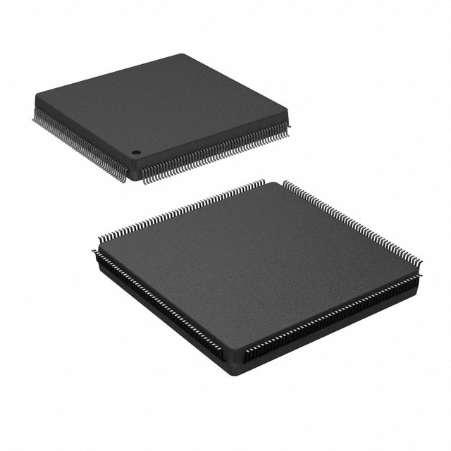
Package
XC2C256-6PQ208C is available in a PQ208 package, which refers to a plastic quad flat pack with 208 pins.
Essence
The essence of XC2C256-6PQ208C lies in its ability to provide a reconfigurable hardware platform that allows users to implement custom digital logic designs without the need for dedicated integrated circuits.
Packaging/Quantity
XC2C256-6PQ208C is typically packaged individually and is available in varying quantities depending on the supplier or manufacturer.
Specifications
- Logic Cells: 256
- CLB Flip-Flops: 4,096
- Maximum User I/Os: 173
- Maximum Distributed RAM: 32,768 bits
- Maximum Distributed ROM: 32,768 bits
- Maximum Global Clock Frequency: 200 MHz
- Operating Voltage: 3.3V
- Package Type: PQ208
Detailed Pin Configuration
The pin configuration of XC2C256-6PQ208C is as follows:
- Pin 1: VCCIO
- Pin 2: GND
- Pin 3: IOL1N0
- Pin 4: IOL1P0
- Pin 5: IOL1N1
- Pin 6: IOL1P1
- Pin 7: IOL1N2
- Pin 8: IOL1P2
- Pin 9: IOL1N3
- Pin 10: IOL1P3
- Pin 11: IOL1N4
- Pin 12: IOL1P4
- Pin 13: IOL1N5
- Pin 14: IOL1P5
- Pin 15: IOL1N6
- Pin 16: IOL1P6
- Pin 17: IOL1N7
- Pin 18: IOL1P7
- Pin 19: IOL1N8
- Pin 20: IOL1P8
- Pin 21: IOL1N9
- Pin 22: IOL1P9
- Pin 23: IOL1N10
- Pin 24: IOL1P10
- Pin 25: IOL1N11
- Pin 26: IOL1P11
- Pin 27: IOL1N12
- Pin 28: IOL1P12
- Pin 29: IOL1N13
- Pin 30: IOL1P13
- Pin 31: IOL1N14
- Pin 32: IOL1P14
- Pin 33: IOL1N15
- Pin 34: IOL1P15
- Pin 35: IOL1N16
- Pin 36: IOL1P16
- Pin 37: IOL1N17
- Pin 38: IOL1P17
- Pin 39: IOL1N18
- Pin 40: IOL1P18
- Pin 41: IOL1N19
- Pin 42: IOL1P19
- Pin 43: IOL1N20
- Pin 44: IOL1P20
- Pin 45: IOL1N21
- Pin 46: IOL1P21
- Pin 47: IO_L1N
Enumere 10 preguntas y respuestas comunes relacionadas con la aplicación de XC2C256-6PQ208C en soluciones técnicas
Sure! Here are 10 common questions and answers related to the application of XC2C256-6PQ208C in technical solutions:
Question: What is XC2C256-6PQ208C?
- Answer: XC2C256-6PQ208C is a field-programmable gate array (FPGA) manufactured by Xilinx. It offers 256 macrocells and operates at a speed grade of -6.Question: What are the typical applications of XC2C256-6PQ208C?
- Answer: XC2C256-6PQ208C can be used in various applications such as digital signal processing, embedded systems, communication systems, industrial automation, and more.Question: What is the maximum operating frequency of XC2C256-6PQ208C?
- Answer: The maximum operating frequency of XC2C256-6PQ208C depends on the design and implementation, but it can typically reach frequencies up to 200 MHz.Question: How much logic can XC2C256-6PQ208C accommodate?
- Answer: XC2C256-6PQ208C has 256 macrocells, which can be used to implement various types of logic functions, including combinational and sequential circuits.Question: Can XC2C256-6PQ208C interface with external devices?
- Answer: Yes, XC2C256-6PQ208C supports various I/O standards and can interface with external devices such as sensors, memory modules, communication interfaces, and more.Question: What development tools are available for programming XC2C256-6PQ208C?
- Answer: Xilinx provides software tools like Vivado or ISE Design Suite that allow users to design, simulate, and program XC2C256-6PQ208C.Question: Can XC2C256-6PQ208C be reprogrammed?
- Answer: Yes, XC2C256-6PQ208C is a field-programmable device, which means it can be reprogrammed multiple times to implement different designs or functionalities.Question: What power supply voltage does XC2C256-6PQ208C require?
- Answer: XC2C256-6PQ208C typically operates at a voltage of 3.3V, but it also supports lower voltages depending on the specific requirements of the application.Question: Is XC2C256-6PQ208C suitable for high-speed applications?
- Answer: Yes, XC2C256-6PQ208C can be used in high-speed applications as it offers a range of features like fast carry logic, dedicated clock resources, and advanced routing capabilities.Question: Are there any limitations or considerations when using XC2C256-6PQ208C?
- Answer: Some considerations include power consumption, heat dissipation, I/O voltage compatibility, and the need for proper grounding and decoupling techniques to ensure reliable operation.
Please note that these answers are general and may vary based on specific design requirements and implementation details.