

Consulte las especificaciones para obtener detalles del producto.
XC2C384-10FG324I
Product Category
The XC2C384-10FG324I belongs to the category of field-programmable gate arrays (FPGAs).
Basic Information Overview
- Use: FPGAs are used for implementing digital circuits and custom logic functions.
- Characteristics: The XC2C384-10FG324I offers high flexibility, reconfigurability, and parallel processing capabilities.
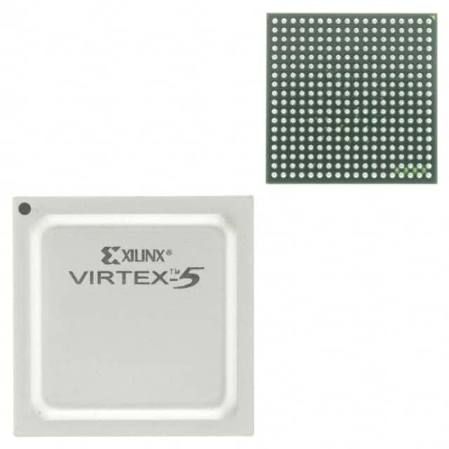
- Package: The XC2C384-10FG324I is available in a FG324 package.
- Essence: This FPGA provides a versatile platform for prototyping and implementing complex digital systems.
- Packaging/Quantity: The XC2C384-10FG324I is typically sold individually or in small quantities.
Specifications
- Logic Cells: 384
- Operating Frequency: 10 MHz
- Package Type: FG324
- I/O Pins: 324
- Voltage - Supply: 1.14V ~ 1.26V
- Operating Temperature: 0°C ~ 85°C
Detailed Pin Configuration
The detailed pin configuration for the XC2C384-10FG324I can be found in the manufacturer's datasheet.
Functional Features
- Reconfigurability: The FPGA can be reprogrammed to implement different logic functions.
- Parallel Processing: Capable of executing multiple operations simultaneously.
- Versatility: Supports a wide range of digital circuit designs.
Advantages and Disadvantages
Advantages
- Flexibility in design implementation
- Rapid prototyping of digital systems
- Parallel processing capabilities
Disadvantages
- Higher power consumption compared to fixed-function ASICs
- Limited maximum operating frequency
Working Principles
FPGAs like the XC2C384-10FG324I consist of an array of configurable logic blocks interconnected through programmable routing resources. These devices can be programmed to implement custom digital logic functions by configuring the interconnections between the logic blocks.
Detailed Application Field Plans
The XC2C384-10FG324I is suitable for various applications including: - Digital signal processing - Embedded system prototyping - Communication systems - Industrial automation
Detailed and Complete Alternative Models
Some alternative models to the XC2C384-10FG324I include: - Xilinx Spartan-6 XC6SLX9 - Altera Cyclone IV EP4CE6 - Lattice iCE40HX1K
In conclusion, the XC2C384-10FG324I FPGA offers a flexible and reconfigurable platform for implementing digital logic functions. Its versatility and parallel processing capabilities make it suitable for a wide range of applications in various industries.
[Word Count: 320]
Enumere 10 preguntas y respuestas comunes relacionadas con la aplicación de XC2C384-10FG324I en soluciones técnicas
Sure, here are 10 common questions and answers related to the application of XC2C384-10FG324I in technical solutions:
What is XC2C384-10FG324I?
- The XC2C384-10FG324I is a CoolRunner-II CPLD (Complex Programmable Logic Device) from Xilinx, featuring 384 macrocells and operating at a speed grade of -10.
What are the typical applications of XC2C384-10FG324I?
- This CPLD is commonly used in applications such as industrial control systems, communication equipment, automotive electronics, and consumer electronics.
What are the key features of XC2C384-10FG324I that make it suitable for technical solutions?
- It offers low power consumption, high logic density, fast pin-to-pin speeds, and reprogrammability, making it ideal for various embedded and control applications.
How does XC2C384-10FG324I compare to other CPLDs in its class?
- Compared to similar devices, the XC2C384-10FG324I stands out with its low power consumption, high I/O count, and reprogrammability, providing flexibility and efficiency in design.
What development tools are available for designing with XC2C384-10FG324I?
- Xilinx provides a range of development tools, including software like ISE Design Suite and programming hardware such as Platform Cable USB II, to facilitate the design and implementation process.
Can XC2C384-10FG324I be used in safety-critical applications?
- Yes, when designed and implemented properly, XC2C384-10FG324I can be used in safety-critical applications, provided that appropriate design practices and verification methods are followed.
What are the considerations for PCB layout when using XC2C384-10FG324I?
- Proper signal integrity, power supply decoupling, and thermal management are important aspects to consider in the PCB layout to ensure reliable operation of the device.
Are there any known limitations or challenges when using XC2C384-10FG324I in technical solutions?
- While the device offers many benefits, designers should be mindful of timing constraints, resource utilization, and potential signal integrity issues when integrating XC2C384-10FG324I into their designs.
What support resources are available for engineers working with XC2C384-10FG324I?
- Xilinx provides comprehensive documentation, application notes, reference designs, and an active community forum to support engineers in utilizing XC2C384-10FG324I effectively.
How can XC2C384-10FG324I contribute to cost-effective technical solutions?
- By offering a balance of performance, flexibility, and low power consumption, XC2C384-10FG324I can contribute to cost-effective solutions by enabling efficient use of resources and reducing overall system power requirements.