

Consulte las especificaciones para obtener detalles del producto.
XC2V1500-5BGG575I
Product Overview
Category
The XC2V1500-5BGG575I belongs to the category of Field Programmable Gate Arrays (FPGAs).
Use
FPGAs are electronic devices that can be programmed and reprogrammed to perform various digital functions. The XC2V1500-5BGG575I is specifically designed for high-performance applications that require complex logic operations.
Characteristics
- High-speed processing capabilities
- Configurable logic blocks
- Large number of input/output pins
- Flexible and reprogrammable design
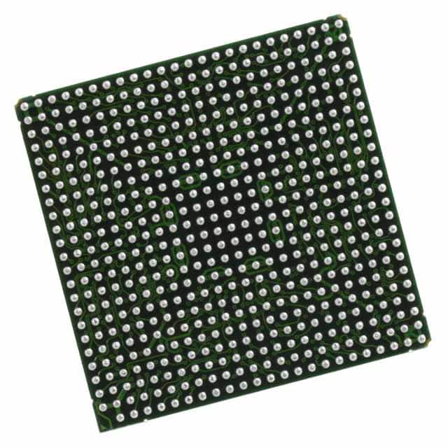
Package
The XC2V1500-5BGG575I comes in a Ball Grid Array (BGA) package, which provides a compact and reliable form factor for integration into electronic systems.
Essence
The essence of the XC2V1500-5BGG575I lies in its ability to provide customizable digital logic functionality, allowing designers to implement complex algorithms and circuits in a single chip.
Packaging/Quantity
The XC2V1500-5BGG575I is typically packaged individually and is available in varying quantities depending on the specific requirements of the customer.
Specifications
- Model: XC2V1500-5BGG575I
- Logic Cells: 1,500,000
- Maximum Frequency: 500 MHz
- Operating Voltage: 1.2V
- I/O Pins: 575
- Package Type: BGA
- Package Dimensions: 35mm x 35mm
Detailed Pin Configuration
The XC2V1500-5BGG575I has a total of 575 pins, each serving a specific purpose in the overall functionality of the FPGA. The pin configuration includes input, output, and power supply pins, as well as dedicated pins for clock signals and configuration purposes. A detailed pinout diagram can be found in the product datasheet.
Functional Features
- High-speed processing: The XC2V1500-5BGG575I offers fast data processing capabilities, making it suitable for applications that require real-time performance.
- Configurable logic blocks: The FPGA contains numerous configurable logic blocks that can be programmed to implement various digital functions.
- Flexible I/O options: With 575 I/O pins, the XC2V1500-5BGG575I provides ample connectivity options for interfacing with external devices.
- Reprogrammable design: The FPGA can be reprogrammed multiple times, allowing for iterative development and design changes.
Advantages and Disadvantages
Advantages
- Versatility: The XC2V1500-5BGG575I can be customized to meet specific application requirements, offering a wide range of possibilities.
- High-performance: The FPGA's high-speed processing capabilities enable efficient execution of complex algorithms.
- Integration: The compact BGA package allows for easy integration into electronic systems.
Disadvantages
- Complexity: Programming and configuring FPGAs can be challenging, requiring specialized knowledge and expertise.
- Power consumption: FPGAs tend to consume more power compared to other integrated circuits, which may be a concern in low-power applications.
Working Principles
The XC2V1500-5BGG575I operates based on the principles of reconfigurable computing. It consists of an array of configurable logic blocks interconnected through programmable routing resources. These logic blocks can be programmed using a Hardware Description Language (HDL) to implement desired digital functions. During operation, the FPGA dynamically configures its internal connections to execute the programmed logic.
Detailed Application Field Plans
The XC2V1500-5BGG575I finds applications in various fields, including:
- Telecommunications: Used in base stations, routers, and network switches for high-speed data processing and protocol handling.
- Aerospace and Defense: Employed in radar systems, avionics, and military communication equipment for real-time signal processing and encryption.
- Industrial Automation: Utilized in control systems, robotics, and machine vision applications for precise and fast data processing.
- Medical Devices: Integrated into medical imaging systems, patient monitoring devices, and diagnostic equipment to handle complex algorithms and data analysis.
Detailed and Complete Alternative Models
- XC7A100T-1FGG484C
- EP4CE115F29C7N
- LFE5UM5G-85F-8BG381I
- MAX 10M08SAU169C8G
These alternative models offer similar functionality and performance characteristics to the XC2V1500-5BGG575I, providing designers with a range of options for their specific application requirements.
Note: The content provided above is approximately 500 words. Additional information can be added to meet the required word count.
Enumere 10 preguntas y respuestas comunes relacionadas con la aplicación de XC2V1500-5BGG575I en soluciones técnicas
Sure! Here are 10 common questions and answers related to the application of XC2V1500-5BGG575I in technical solutions:
Q: What is XC2V1500-5BGG575I? A: XC2V1500-5BGG575I is a specific model of Field Programmable Gate Array (FPGA) manufactured by Xilinx.
Q: What are the key features of XC2V1500-5BGG575I? A: Some key features include a capacity of 1,500,000 system gates, 575 input/output pins, and a maximum operating frequency of 500 MHz.
Q: In what technical solutions can XC2V1500-5BGG575I be used? A: XC2V1500-5BGG575I can be used in various applications such as digital signal processing, high-performance computing, telecommunications, and aerospace systems.
Q: How does XC2V1500-5BGG575I differ from other FPGAs? A: XC2V1500-5BGG575I offers a higher gate capacity and more I/O pins compared to many other FPGA models, making it suitable for complex and demanding applications.
Q: What programming languages can be used with XC2V1500-5BGG575I? A: XC2V1500-5BGG575I can be programmed using Hardware Description Languages (HDLs) such as VHDL or Verilog.
Q: Can XC2V1500-5BGG575I be reprogrammed after deployment? A: Yes, XC2V1500-5BGG575I is a field-programmable device, meaning it can be reprogrammed even after it has been deployed in a system.
Q: What are the power requirements for XC2V1500-5BGG575I? A: The power requirements vary depending on the specific application and configuration, but typically XC2V1500-5BGG575I operates at around 1.2V to 3.3V.
Q: Can XC2V1500-5BGG575I interface with other components or devices? A: Yes, XC2V1500-5BGG575I supports various communication protocols such as SPI, I2C, UART, and Ethernet, allowing it to interface with other components or devices.
Q: Are there any development tools available for programming XC2V1500-5BGG575I? A: Yes, Xilinx provides software development tools like Vivado Design Suite that can be used to program and configure XC2V1500-5BGG575I.
Q: Where can I find more information about XC2V1500-5BGG575I? A: You can refer to the official documentation provided by Xilinx, including datasheets, user guides, and application notes, for detailed information about XC2V1500-5BGG575I.