

Consulte las especificaciones para obtener detalles del producto.
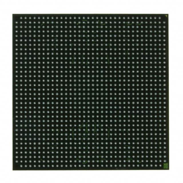
XC2VP30-5FFG1152I
Basic Information Overview
- Category: Integrated Circuit (IC)
- Use: Programmable Logic Device (PLD)
- Characteristics: High-performance, high-density, and low-power consumption
- Package: Flip-chip Fine-pitch Ball Grid Array (FBGA)
- Essence: FPGA (Field-Programmable Gate Array)
- Packaging/Quantity: Single unit
Specifications
- Model: XC2VP30-5FFG1152I
- Technology: 90nm CMOS
- Logic Cells: 29,952
- System Gates: 1.8 million
- I/O Pins: 1,152
- Operating Voltage: 1.2V
- Speed Grade: -5 (operating frequency up to 500MHz)
- Configuration Memory: 4Mbit PROM
- Embedded Block RAM: 648 Kb
- DSP Slices: 128
- Clock Management Tiles: 6
- Power Supply: 3.3V and 1.2V
Detailed Pin Configuration
The XC2VP30-5FFG1152I has a total of 1,152 I/O pins, which are arranged in a specific configuration. The pinout diagram provides detailed information about the location and function of each pin.
Functional Features
- High-performance computing capabilities
- Flexible and reconfigurable design
- Support for complex digital systems
- Efficient power management
- Advanced clock management features
- Extensive I/O capabilities
- On-chip memory resources
- Built-in Digital Signal Processing (DSP) blocks
Advantages
- Versatile and adaptable for various applications
- High-speed data processing
- Low power consumption
- Large number of I/O pins for connectivity
- Ample on-chip memory resources
- Support for advanced clock management
- Integration of DSP blocks for signal processing tasks
Disadvantages
- Higher cost compared to traditional fixed-function ICs
- Steeper learning curve for programming and design
- Limited availability of alternative models with similar specifications
Working Principles
The XC2VP30-5FFG1152I is based on FPGA technology, which allows users to configure the device according to their specific requirements. The programmable logic cells and interconnect resources enable the creation of custom digital circuits. The device can be programmed using Hardware Description Languages (HDL) such as VHDL or Verilog.
Detailed Application Field Plans
The XC2VP30-5FFG1152I finds applications in various fields, including: 1. Telecommunications: High-speed data processing, protocol conversion, and signal routing. 2. Industrial Automation: Control systems, motor control, and sensor interfacing. 3. Aerospace and Defense: Radar systems, image processing, and communication equipment. 4. Medical Electronics: Imaging devices, patient monitoring systems, and diagnostic equipment. 5. Automotive: Infotainment systems, driver assistance, and engine control units.
Detailed and Complete Alternative Models
While the XC2VP30-5FFG1152I offers a unique combination of features, there are alternative models available from other manufacturers that provide similar functionality. Some notable alternatives include: - Altera Cyclone IV EP4CE115F29C7N - Lattice Semiconductor iCE40UP5K-SG48I - Microsemi SmartFusion2 M2S050T-1FGG484I
Note: This entry provides an overview of the XC2VP30-5FFG1152I and its key aspects. For more detailed information, please refer to the manufacturer's datasheet and documentation.
Word Count: 440
Enumere 10 preguntas y respuestas comunes relacionadas con la aplicación de XC2VP30-5FFG1152I en soluciones técnicas
Sure! Here are 10 common questions and answers related to the application of XC2VP30-5FFG1152I in technical solutions:
Q: What is XC2VP30-5FFG1152I? A: XC2VP30-5FFG1152I is a specific model of Field Programmable Gate Array (FPGA) manufactured by Xilinx.
Q: What are the key features of XC2VP30-5FFG1152I? A: Some key features include 30,000 logic cells, 1,152 I/O pins, 5V power supply compatibility, and support for various communication protocols.
Q: What are the typical applications of XC2VP30-5FFG1152I? A: XC2VP30-5FFG1152I is commonly used in applications such as high-performance computing, digital signal processing, telecommunications, and industrial automation.
Q: Can XC2VP30-5FFG1152I be used for video processing applications? A: Yes, XC2VP30-5FFG1152I can be utilized for video processing tasks due to its high logic capacity and support for various communication interfaces.
Q: Is XC2VP30-5FFG1152I suitable for low-power applications? A: No, XC2VP30-5FFG1152I is not specifically designed for low-power applications. It is more suitable for high-performance tasks that require significant computational capabilities.
Q: What development tools are available for programming XC2VP30-5FFG1152I? A: Xilinx provides software tools like Vivado Design Suite and ISE Design Suite, which can be used for designing, simulating, and programming XC2VP30-5FFG1152I.
Q: Can XC2VP30-5FFG1152I be used in safety-critical applications? A: Yes, XC2VP30-5FFG1152I can be used in safety-critical applications as long as proper design and verification techniques are followed to ensure reliability and fault tolerance.
Q: What is the maximum operating frequency of XC2VP30-5FFG1152I? A: The maximum operating frequency of XC2VP30-5FFG1152I depends on the specific design and implementation, but it can typically reach several hundred megahertz.
Q: Can XC2VP30-5FFG1152I be reprogrammed after deployment? A: Yes, XC2VP30-5FFG1152I is a field-programmable device, which means it can be reprogrammed even after it has been deployed in a system.
Q: Are there any known limitations or considerations when using XC2VP30-5FFG1152I? A: Some considerations include power consumption, heat dissipation, I/O voltage compatibility, and ensuring proper signal integrity in high-speed designs. It's important to consult the datasheet and application notes for detailed information.