

Consulte las especificaciones para obtener detalles del producto.
XC2VP70-5FFG1517I
Product Overview
Category
XC2VP70-5FFG1517I belongs to the category of Field Programmable Gate Arrays (FPGAs).
Use
This FPGA is commonly used in various electronic applications that require high-performance digital logic circuits.
Characteristics
- High-speed processing capabilities
- Configurable and reprogrammable
- Large number of programmable logic cells
- Flexible I/O options
- Low power consumption
Package
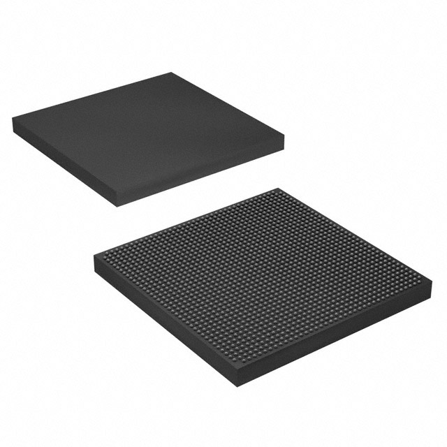
XC2VP70-5FFG1517I is available in a Flip Chip FineLine BGA package.
Essence
The essence of XC2VP70-5FFG1517I lies in its ability to provide customizable digital logic circuits, enabling designers to implement complex functionalities in electronic systems.
Packaging/Quantity
XC2VP70-5FFG1517I is typically packaged individually and is available in varying quantities depending on customer requirements.
Specifications
- FPGA Family: Virtex-II Pro
- Logic Cells: 70,000
- System Gates: 1.5 million
- Block RAM: 864 Kb
- DSP Slices: 192
- Maximum Frequency: 500 MHz
- Operating Voltage: 1.8V
- I/O Standards: LVCMOS, LVTTL, HSTL, SSTL, LVDS, RSDS
Detailed Pin Configuration
The detailed pin configuration for XC2VP70-5FFG1517I can be found in the product datasheet provided by the manufacturer.
Functional Features
- High-speed data processing
- Configurable logic cells for custom functionality
- On-chip memory blocks for efficient data storage
- Dedicated DSP slices for signal processing tasks
- Flexible I/O options for interfacing with external devices
- Built-in clock management resources for precise timing control
Advantages and Disadvantages
Advantages
- High-performance FPGA with large logic capacity
- Configurable and reprogrammable, allowing for design flexibility
- Low power consumption compared to alternative solutions
- Wide range of I/O standards supported for versatile interfacing
Disadvantages
- Relatively higher cost compared to other programmable logic devices
- Steeper learning curve for inexperienced designers
- Limited availability of alternative models with similar specifications
Working Principles
XC2VP70-5FFG1517I operates based on the principles of digital logic circuits. It consists of a large number of configurable logic cells interconnected through programmable routing resources. These logic cells can be programmed to implement desired functionality by configuring their internal look-up tables and flip-flops.
The FPGA is programmed using hardware description languages (HDL) such as VHDL or Verilog. The design is synthesized, mapped, and then loaded onto the FPGA using specialized software tools. Once programmed, the FPGA executes the desired functionality by routing signals through the configured logic cells.
Detailed Application Field Plans
XC2VP70-5FFG1517I finds applications in various fields, including:
- Telecommunications: Used in high-speed data transmission systems, network routers, and switches.
- Aerospace and Defense: Employed in radar systems, avionics, and military communication equipment.
- Industrial Automation: Utilized in control systems, robotics, and machine vision applications.
- Medical Electronics: Applied in medical imaging devices, patient monitoring systems, and diagnostic equipment.
- Automotive: Used in advanced driver assistance systems (ADAS), infotainment systems, and engine control units (ECUs).
Detailed and Complete Alternative Models
While XC2VP70-5FFG1517I offers unique features and specifications, there are alternative FPGA models available in the market that cater to similar requirements. Some notable alternatives include:
- Xilinx Virtex-7 XC7VX690T: Offers higher logic capacity and improved performance.
- Intel Stratix 10 GX: Provides advanced features like high-speed transceivers and embedded memory.
- Lattice ECP5: Offers a cost-effective solution with low power consumption.
These alternative models can be considered based on specific project requirements and budget constraints.
In conclusion, XC2VP70-5FFG1517I is a high-performance FPGA belonging to the Virtex-II Pro family. It offers configurable logic cells, flexible I/O options, and low power consumption. While it has advantages such as design flexibility and high-speed processing, it also has disadvantages like higher cost and limited availability of alternative models. Its working principle involves configuring logic cells through hardware description languages. This FPGA finds applications in telecommunications, aerospace, industrial automation, medical electronics, and automotive sectors. Alternative models like Xilinx Virtex-7 XC7VX690T, Intel Stratix 10 GX, and Lattice ECP5 provide additional options for designers.
Enumere 10 preguntas y respuestas comunes relacionadas con la aplicación de XC2VP70-5FFG1517I en soluciones técnicas
Sure! Here are 10 common questions and answers related to the application of XC2VP70-5FFG1517I in technical solutions:
Question: What is XC2VP70-5FFG1517I?
- Answer: XC2VP70-5FFG1517I is a specific model of Field Programmable Gate Array (FPGA) manufactured by Xilinx.Question: What are the key features of XC2VP70-5FFG1517I?
- Answer: Some key features of XC2VP70-5FFG1517I include 70,000 logic cells, 1.2V core voltage, 5-speed grade, and a 1517-pin Fine-Pitch Ball Grid Array (FBGA) package.Question: What are the typical applications of XC2VP70-5FFG1517I?
- Answer: XC2VP70-5FFG1517I is commonly used in various technical solutions such as high-performance computing, digital signal processing, telecommunications, and aerospace systems.Question: Can XC2VP70-5FFG1517I be used for real-time video processing?
- Answer: Yes, XC2VP70-5FFG1517I can be used for real-time video processing due to its high logic capacity and performance capabilities.Question: Is XC2VP70-5FFG1517I suitable for low-power applications?
- Answer: No, XC2VP70-5FFG1517I is not specifically designed for low-power applications. It is more suitable for high-performance applications that require significant computational power.Question: What development tools are available for programming XC2VP70-5FFG1517I?
- Answer: Xilinx provides various development tools such as Vivado Design Suite and ISE Design Suite for programming and configuring XC2VP70-5FFG1517I.Question: Can XC2VP70-5FFG1517I be used in a multi-FPGA system?
- Answer: Yes, XC2VP70-5FFG1517I can be used in a multi-FPGA system by connecting multiple FPGAs together using appropriate communication interfaces.Question: What is the maximum clock frequency supported by XC2VP70-5FFG1517I?
- Answer: The maximum clock frequency supported by XC2VP70-5FFG1517I depends on the specific design and implementation, but it can typically reach several hundred megahertz (MHz) or even gigahertz (GHz).Question: Are there any specific design considerations when using XC2VP70-5FFG1517I?
- Answer: Yes, when designing with XC2VP70-5FFG1517I, factors like power consumption, thermal management, signal integrity, and timing constraints should be carefully considered.Question: Can XC2VP70-5FFG1517I be reprogrammed after deployment?
- Answer: Yes, XC2VP70-5FFG1517I is a Field Programmable Gate Array, which means it can be reprogrammed even after it has been deployed in a technical solution.
Please note that the answers provided here are general and may vary depending on the specific requirements and context of the application.