

Consulte las especificaciones para obtener detalles del producto.
XC3S250E-4VQG100I
Product Overview
Category
The XC3S250E-4VQG100I belongs to the category of Field-Programmable Gate Arrays (FPGAs).
Use
FPGAs are integrated circuits that can be programmed after manufacturing. They are widely used in various electronic applications, including telecommunications, automotive, aerospace, and consumer electronics.
Characteristics
- The XC3S250E-4VQG100I is a high-performance FPGA with advanced features.
- It offers a large number of configurable logic blocks and programmable interconnects.
- The device supports various I/O standards and has built-in memory resources.
- It provides flexibility and reconfigurability, allowing for rapid prototyping and design iterations.
Package
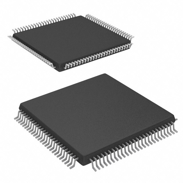
The XC3S250E-4VQG100I comes in a Quad Flat No-Lead (QFN) package.
Essence
The essence of the XC3S250E-4VQG100I lies in its ability to provide a customizable hardware platform for implementing digital logic designs.
Packaging/Quantity
The XC3S250E-4VQG100I is typically packaged in reels or trays, with a quantity of 100 units per package.
Specifications
- Logic Cells: 250,000
- Block RAM: 1,152 Kbits
- DSP Slices: 240
- Maximum Frequency: 400 MHz
- Operating Voltage: 1.2V
- Package Type: QFN
- Temperature Range: -40°C to +100°C
Detailed Pin Configuration
The XC3S250E-4VQG100I has a total of 100 pins. The pin configuration is as follows:
(Pin Number) - (Pin Name) 1 - VCCINT 2 - GND 3 - IOL1PT0AD0N14 4 - IOL1NT0AD0P14 5 - IOL2PT0AD1N14 6 - IOL2NT0AD1P14 7 - IOL3PT0AD2N14 8 - IOL3NT0AD2P14 9 - IOL4PT0AD3N14 10 - IOL4NT0AD3P14 ... 100 - GND
Functional Features
- High-performance FPGA with advanced architecture.
- Configurable logic blocks for implementing complex digital designs.
- Programmable interconnects for flexible routing of signals.
- Built-in memory resources for data storage and processing.
- Support for various I/O standards for interfacing with external devices.
Advantages and Disadvantages
Advantages
- Flexibility and reconfigurability enable rapid prototyping and design iterations.
- High-performance capabilities suitable for demanding applications.
- Large number of logic cells and memory resources provide ample resources for complex designs.
- Wide range of supported I/O standards allows for versatile interfacing options.
Disadvantages
- FPGAs can be more expensive compared to other types of integrated circuits.
- Designing and programming FPGAs require specialized knowledge and tools.
- Power consumption of FPGAs can be relatively high compared to dedicated ASICs.
Working Principles
The XC3S250E-4VQG100I operates based on the principles of configurable logic and programmable interconnects. The device consists of a matrix of configurable logic blocks interconnected through programmable routing resources. These logic blocks can be programmed to implement desired digital functions, while the interconnects allow for the routing of signals between different blocks. The configuration of the FPGA is stored in non-volatile memory and can be reprogrammed as needed.
Detailed Application Field Plans
The XC3S250E-4VQG100I finds applications in various fields, including:
- Telecommunications: Used for implementing high-speed data processing and signal routing in communication systems.
- Automotive: Employed in automotive electronics for functions such as engine control, driver assistance systems, and infotainment.
- Aerospace: Utilized in aerospace applications for tasks like flight control, navigation, and satellite communication.
- Consumer Electronics: Integrated into consumer electronic devices like smartphones, tablets, and gaming consoles for enhanced functionality and performance.
Detailed and Complete Alternative Models
- XC3S500E-4FG320C: A higher-capacity FPGA with 500,000 logic cells and 1,536 Kbits of block RAM.
- XC3S1000E-4FG320C: An even larger FPGA with 1,000,000 logic cells and 2,304 Kbits of block RAM.
- XC3S2000E-4FG320C: A top-of-the-line FPGA with
Enumere 10 preguntas y respuestas comunes relacionadas con la aplicación de XC3S250E-4VQG100I en soluciones técnicas
Sure! Here are 10 common questions and answers related to the application of XC3S250E-4VQG100I in technical solutions:
Question: What is XC3S250E-4VQG100I?
- Answer: XC3S250E-4VQG100I is a specific model of Field-Programmable Gate Array (FPGA) manufactured by Xilinx.Question: What are the key features of XC3S250E-4VQG100I?
- Answer: Some key features include 250,000 system gates, 192 user I/Os, 16 multipliers, and 8 digital clock managers.Question: What are the typical applications of XC3S250E-4VQG100I?
- Answer: XC3S250E-4VQG100I is commonly used in various technical solutions such as industrial automation, telecommunications, automotive electronics, and medical devices.Question: How can XC3S250E-4VQG100I be programmed?
- Answer: XC3S250E-4VQG100I can be programmed using Xilinx's Vivado Design Suite or other compatible programming tools.Question: Can XC3S250E-4VQG100I be reprogrammed after initial programming?
- Answer: Yes, XC3S250E-4VQG100I is a reprogrammable FPGA, allowing for flexibility in design iterations and updates.Question: What is the power supply requirement for XC3S250E-4VQG100I?
- Answer: The recommended power supply voltage for XC3S250E-4VQG100I is typically 1.2V, but it can operate within a range of 1.14V to 1.26V.Question: Can XC3S250E-4VQG100I interface with other components or devices?
- Answer: Yes, XC3S250E-4VQG100I supports various communication protocols such as SPI, I2C, UART, and Ethernet, allowing for seamless integration with other components or devices.Question: What is the maximum operating frequency of XC3S250E-4VQG100I?
- Answer: The maximum operating frequency of XC3S250E-4VQG100I depends on the specific design and implementation, but it can typically reach frequencies in the range of several hundred megahertz (MHz).Question: Are there any development boards available for XC3S250E-4VQG100I?
- Answer: Yes, Xilinx provides development boards specifically designed for XC3S250E-4VQG100I, which can aid in prototyping and testing.Question: Where can I find additional resources and support for XC3S250E-4VQG100I?
- Answer: Xilinx's official website offers comprehensive documentation, application notes, forums, and technical support for XC3S250E-4VQG100I.