

Consulte las especificaciones para obtener detalles del producto.
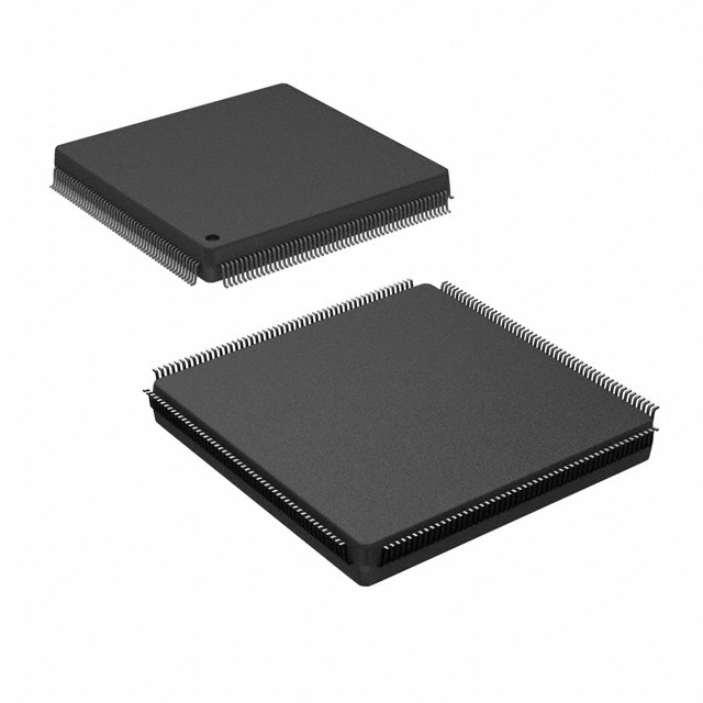
XC3S400-4PQG208I
Basic Information Overview
- Category: Integrated Circuit (IC)
- Use: Programmable Logic Device (PLD)
- Characteristics: High-performance, low-power FPGA (Field-Programmable Gate Array)
- Package: PQG208
- Essence: The XC3S400-4PQG208I is a member of the Spartan-3 family of FPGAs developed by Xilinx.
- Packaging/Quantity: Available in tape and reel packaging, with a quantity of 250 units per reel.
Specifications
The XC3S400-4PQG208I offers the following specifications: - Logic Cells: 400 - CLB Flip-Flops: 2,400 - Block RAM: 12,288 bits - Maximum Frequency: 500 MHz - I/O Pins: 173 - Operating Voltage: 1.2V - Operating Temperature Range: -40°C to +100°C
Detailed Pin Configuration
The XC3S400-4PQG208I has a pin configuration as follows:
| Pin Number | Pin Name | Description | |------------|----------|-------------| | 1 | VCCINT | Internal core voltage supply | | 2 | GND | Ground | | 3 | TCK | JTAG Test Clock | | ... | ... | ... | | 208 | TDI | JTAG Test Data In |
Functional Features
The XC3S400-4PQG208I offers several functional features, including: - Configurable logic blocks (CLBs) for implementing combinatorial and sequential logic functions. - Dedicated digital clock managers (DCMs) for precise clock generation and distribution. - Built-in multipliers for efficient implementation of arithmetic operations. - SelectIO technology for flexible I/O voltage standards and signaling levels. - On-chip memory blocks for data storage and retrieval.
Advantages and Disadvantages
Advantages of the XC3S400-4PQG208I include: - High-performance FPGA with a maximum frequency of 500 MHz. - Low-power consumption, making it suitable for battery-powered applications. - Flexible I/O voltage standards and signaling levels. - Large number of logic cells and flip-flops for complex designs.
Disadvantages of the XC3S400-4PQG208I include: - Limited amount of on-chip memory compared to some other FPGAs. - Relatively high cost compared to lower-end FPGAs. - Requires specialized knowledge and tools for programming and configuration.
Working Principles
The XC3S400-4PQG208I is based on the concept of reconfigurable hardware. It consists of an array of configurable logic blocks (CLBs) interconnected through programmable interconnects. These CLBs can be programmed to implement various logic functions, allowing the device to perform different tasks based on the user's requirements. The configuration of the FPGA is stored in non-volatile memory and can be reprogrammed as needed.
Detailed Application Field Plans
The XC3S400-4PQG208I finds applications in various fields, including: 1. Communications: Used in wireless base stations, network routers, and communication protocols. 2. Industrial Automation: Employed in control systems, motor drives, and sensor interfaces. 3. Aerospace and Defense: Utilized in radar systems, avionics, and secure communications. 4. Medical Devices: Integrated into medical imaging equipment, patient monitoring systems, and laboratory instruments. 5. Automotive: Applied in automotive electronics, driver assistance systems, and infotainment systems.
Detailed and Complete Alternative Models
Alternative models to the XC3S400-4PQG208I include: 1. XC3S50-4VQG100C: A smaller FPGA with 50 logic cells and 100-pin VQG package. 2. XC3S200-4FT256I: A larger FPGA with 200 logic cells and 256-pin FT256 package. 3. XC3S1000-4FG456C: A higher-end FPGA with 1000 logic cells and 456-pin FG456 package.
These alternative models offer different levels of performance, capacity, and packaging options to suit various design requirements.
In conclusion, the XC3S400-4PQG208I is a high-performance, low-power FPGA belonging to the Spartan-3 family. It offers a range of functional features, advantages, and disadvantages, making it suitable for diverse applications in fields such as communications, industrial automation, aerospace, medical devices, and automotive. Alternative models provide flexibility in terms of performance and packaging options.
Enumere 10 preguntas y respuestas comunes relacionadas con la aplicación de XC3S400-4PQG208I en soluciones técnicas
Sure! Here are 10 common questions and answers related to the application of XC3S400-4PQG208I in technical solutions:
Question: What is XC3S400-4PQG208I?
Answer: XC3S400-4PQG208I is a specific model of FPGA (Field-Programmable Gate Array) manufactured by Xilinx.Question: What does XC3S400-4PQG208I offer in terms of technical specifications?
Answer: XC3S400-4PQG208I offers 400,000 system gates, 432 user I/Os, and 4,800 logic cells.Question: How can XC3S400-4PQG208I be used in technical solutions?
Answer: XC3S400-4PQG208I can be used for various applications such as digital signal processing, embedded systems, and high-speed communication.Question: What programming languages can be used to program XC3S400-4PQG208I?
Answer: XC3S400-4PQG208I can be programmed using hardware description languages (HDLs) such as VHDL or Verilog.Question: Can XC3S400-4PQG208I be reprogrammed after it has been initially programmed?
Answer: Yes, XC3S400-4PQG208I is a reprogrammable FPGA, which means it can be reconfigured multiple times.Question: What development tools are available for programming XC3S400-4PQG208I?
Answer: Xilinx provides software tools like Vivado Design Suite that can be used for designing, simulating, and programming XC3S400-4PQG208I.Question: What are the power requirements for XC3S400-4PQG208I?
Answer: XC3S400-4PQG208I typically operates at a voltage range of 1.14V to 1.26V, with a maximum power consumption of around 2.5W.Question: Can XC3S400-4PQG208I interface with other components or devices?
Answer: Yes, XC3S400-4PQG208I supports various communication protocols such as SPI, I2C, UART, and Ethernet, allowing it to interface with other components or devices.Question: Are there any limitations or considerations when using XC3S400-4PQG208I?
Answer: Some considerations include the need for external memory for larger designs, potential power supply noise issues, and the requirement for proper cooling due to its power consumption.Question: Where can I find additional resources or support for working with XC3S400-4PQG208I?
Answer: Xilinx provides documentation, application notes, forums, and technical support to assist users in working with XC3S400-4PQG208I.