

Consulte las especificaciones para obtener detalles del producto.
XC4010E-1PC84C
Product Overview
Category
XC4010E-1PC84C belongs to the category of programmable logic devices (PLDs).
Use
This product is commonly used in digital circuit design and implementation. It provides a flexible and customizable solution for various applications.
Characteristics
- Programmable: The XC4010E-1PC84C can be programmed to perform specific functions, allowing for versatility in circuit design.
- High Integration: This device offers a high level of integration, enabling complex logic circuits to be implemented on a single chip.
- Low Power Consumption: The XC4010E-1PC84C is designed to operate efficiently with low power consumption.
- Fast Operation: With its advanced architecture, this PLD delivers fast operation speeds, making it suitable for time-critical applications.
Package and Quantity
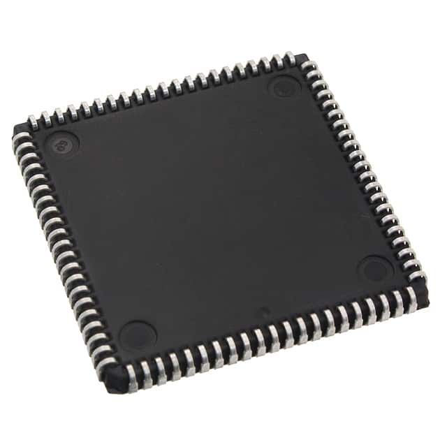
The XC4010E-1PC84C is available in a 84-pin plastic package. Each package contains one unit of the device.
Specifications
- Logic Cells: 400
- Maximum Operating Frequency: 50 MHz
- I/O Pins: 68
- Supply Voltage: 3.3V
- Operating Temperature Range: -40°C to 85°C
Pin Configuration
The detailed pin configuration of XC4010E-1PC84C can be found in the datasheet provided by the manufacturer.
Functional Features
- Flexible Logic Implementation: The XC4010E-1PC84C allows users to implement custom logic functions according to their specific requirements.
- In-system Reprogrammability: This PLD can be reprogrammed while in operation, providing flexibility for design changes or updates.
- Built-in I/O Ports: The device includes a sufficient number of I/O pins to interface with external components or other devices.
- On-chip Memory: The XC4010E-1PC84C incorporates on-chip memory elements, enabling the storage and retrieval of data.
Advantages
- Versatility: The programmable nature of XC4010E-1PC84C allows for a wide range of applications.
- Cost-effective: By eliminating the need for multiple discrete components, this PLD reduces overall system costs.
- Time-saving: With its high integration and reprogrammability, the XC4010E-1PC84C accelerates the design and development process.
Disadvantages
- Limited Resources: The XC4010E-1PC84C has a finite number of logic cells and I/O pins, which may restrict the complexity of designs.
- Learning Curve: Utilizing PLDs requires knowledge of hardware description languages and digital circuit design principles.
Working Principles
The XC4010E-1PC84C operates based on the principles of programmable logic. It consists of configurable logic blocks (CLBs), interconnect resources, and input/output blocks (IOBs). The CLBs can be programmed to implement various logic functions, while the interconnect resources facilitate the routing of signals between different blocks. The IOBs provide interfaces for external connections.
Application Field Plans
The XC4010E-1PC84C finds applications in various fields, including: - Industrial Automation: Control systems, monitoring devices, and data acquisition systems. - Telecommunications: Network switches, routers, and communication equipment. - Consumer Electronics: Set-top boxes, gaming consoles, and multimedia devices. - Automotive: Engine control units, dashboard displays, and safety systems.
Alternative Models
For those seeking alternatives to the XC4010E-1PC84C, the following models offer similar functionality: - XC4000E series by Xilinx - MAX 7000 series by Altera - ATF1500 series by Microchip
In conclusion, the XC4010E-1PC84C is a versatile and programmable logic device that offers high integration, low power consumption, and fast operation. It finds applications in various fields and provides advantages such as cost-effectiveness and time-saving. However, it has limitations in terms of resources and requires expertise in digital circuit design.
Enumere 10 preguntas y respuestas comunes relacionadas con la aplicación de XC4010E-1PC84C en soluciones técnicas
Sure! Here are 10 common questions and answers related to the application of XC4010E-1PC84C in technical solutions:
Q1: What is XC4010E-1PC84C? A1: XC4010E-1PC84C is a specific model of Field-Programmable Gate Array (FPGA) manufactured by Xilinx.
Q2: What is an FPGA? A2: FPGA stands for Field-Programmable Gate Array. It is a type of integrated circuit that can be programmed after manufacturing to perform specific functions.
Q3: What are the key features of XC4010E-1PC84C? A3: Some key features of XC4010E-1PC84C include 4000 logic cells, 84-pin plastic package, and support for various I/O standards.
Q4: What are the typical applications of XC4010E-1PC84C? A4: XC4010E-1PC84C can be used in various applications such as digital signal processing, telecommunications, industrial control systems, and embedded systems.
Q5: How do I program XC4010E-1PC84C? A5: XC4010E-1PC84C can be programmed using Hardware Description Languages (HDLs) like VHDL or Verilog, or through Xilinx's proprietary software tools.
Q6: Can XC4010E-1PC84C be reprogrammed? A6: Yes, XC4010E-1PC84C is a reprogrammable FPGA, which means you can change its functionality by reprogramming it.
Q7: What is the power supply requirement for XC4010E-1PC84C? A7: XC4010E-1PC84C typically requires a 3.3V power supply for its operation.
Q8: Can XC4010E-1PC84C interface with other components or devices? A8: Yes, XC4010E-1PC84C can interface with other components or devices through its I/O pins, which support various standards like LVCMOS, LVTTL, and LVDS.
Q9: Are there any limitations to the XC4010E-1PC84C? A9: XC4010E-1PC84C has a limited number of logic cells and I/O pins, so it may not be suitable for complex designs requiring a large number of resources.
Q10: Where can I find more information about XC4010E-1PC84C? A10: You can refer to the datasheet and technical documentation provided by Xilinx for detailed information about XC4010E-1PC84C, or visit their official website for additional resources.