

Consulte las especificaciones para obtener detalles del producto.
XC4VLX40-10FF1148I
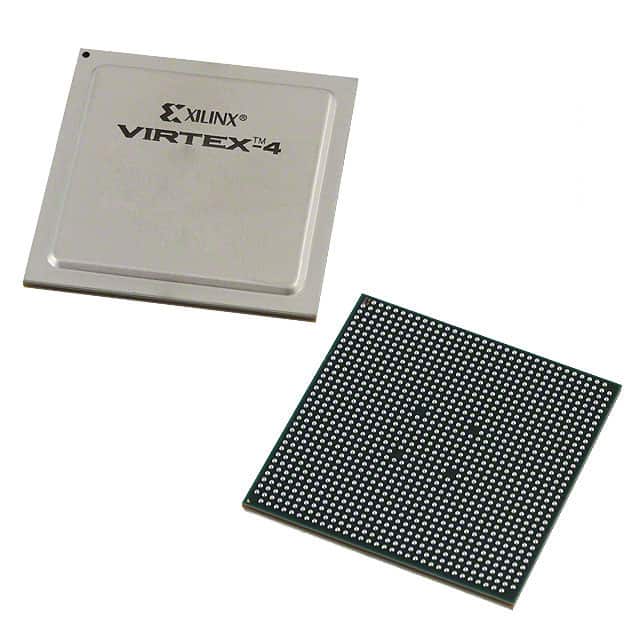
Product Overview
Category
The XC4VLX40-10FF1148I belongs to the category of Field Programmable Gate Arrays (FPGAs).
Use
FPGAs are integrated circuits that can be programmed and reprogrammed to perform various digital functions. The XC4VLX40-10FF1148I is specifically designed for high-performance applications that require complex logic functions.
Characteristics
- High-performance FPGA with advanced features
- Large capacity and flexibility for complex designs
- Low power consumption
- High-speed data processing capabilities
- Support for various communication protocols
- Configurable I/O standards
- Built-in memory blocks for efficient data storage
Package
The XC4VLX40-10FF1148I is available in a Flip-Chip 1148-pin package.
Essence
The essence of the XC4VLX40-10FF1148I lies in its ability to provide a versatile and powerful platform for implementing complex digital designs. It offers a wide range of features and capabilities that make it suitable for demanding applications.
Packaging/Quantity
The XC4VLX40-10FF1148I is typically sold individually or in small quantities, depending on the supplier.
Specifications
- Logic Cells: 40,960
- Block RAM: 1,728 Kbits
- DSP Slices: 160
- Maximum Frequency: 500 MHz
- Operating Voltage: 1.2V
- Operating Temperature Range: -40°C to 100°C
- Configuration Memory: 4Mbit PROM
Detailed Pin Configuration
The XC4VLX40-10FF1148I has a total of 1148 pins, each serving a specific purpose in the overall functionality of the FPGA. A detailed pin configuration diagram can be found in the product datasheet.
Functional Features
- High-speed data processing: The XC4VLX40-10FF1148I offers fast data processing capabilities, making it suitable for applications that require real-time processing.
- Configurable I/O standards: It supports various I/O standards, allowing seamless integration with different devices and interfaces.
- Flexible logic design: With a large number of logic cells, the XC4VLX40-10FF1148I enables the implementation of complex digital designs.
- Built-in memory blocks: The FPGA includes dedicated memory blocks, providing efficient storage for intermediate results and data buffering.
- Support for communication protocols: The XC4VLX40-10FF1148I supports popular communication protocols such as Ethernet, USB, and PCIe, facilitating connectivity with external devices.
Advantages and Disadvantages
Advantages
- High-performance capabilities
- Flexibility in design implementation
- Low power consumption
- Support for various communication protocols
- Large capacity for complex designs
Disadvantages
- Relatively high cost compared to other programmable logic devices
- Steeper learning curve for beginners due to its advanced features
Working Principles
The XC4VLX40-10FF1148I operates based on the principles of reconfigurable computing. It consists of an array of configurable logic blocks interconnected through programmable routing resources. These logic blocks can be programmed to perform specific functions, allowing the FPGA to adapt to different application requirements.
The configuration of the XC4VLX40-10FF1148I is stored in an external memory device, typically a PROM. During startup, the configuration data is loaded into the FPGA, defining the interconnections and functionality of the logic blocks.
Once configured, the XC4VLX40-10FF1148I operates by processing incoming data through the programmed logic blocks, performing the desired operations, and producing the output accordingly.
Detailed Application Field Plans
The XC4VLX40-10FF1148I finds applications in various fields that require high-performance digital processing. Some of the specific application areas include:
- Telecommunications: The FPGA can be used in communication systems for signal processing, protocol conversion, and encryption/decryption.
- Aerospace and Defense: It is suitable for radar systems, avionics, and military-grade communication equipment.
- Industrial Automation: The XC4VLX40-10FF1148I can be utilized in control systems, robotics, and machine vision applications.
- High-Frequency Trading: The FPGA's high-speed data processing capabilities make it ideal for implementing algorithmic trading strategies.
- Medical Imaging: It can be employed in medical imaging devices for real-time image processing and analysis.
Detailed and Complete Alternative Models
- Xilinx Virtex-7 XC7VX485T-2FFG1761C
- Altera Stratix V 5SGXEA7N2F45C2LN
- Lattice ECP5-85F-6BG256C
These alternative models
Enumere 10 preguntas y respuestas comunes relacionadas con la aplicación de XC4VLX40-10FF1148I en soluciones técnicas
Sure! Here are 10 common questions and answers related to the application of XC4VLX40-10FF1148I in technical solutions:
Question: What is XC4VLX40-10FF1148I?
- Answer: XC4VLX40-10FF1148I is a field-programmable gate array (FPGA) manufactured by Xilinx. It is part of the Virtex-4 LX family and has 40,000 logic cells.Question: What are the key features of XC4VLX40-10FF1148I?
- Answer: Some key features of XC4VLX40-10FF1148I include high-performance logic fabric, embedded multipliers, block RAM, built-in DSP slices, and various I/O standards.Question: What are the typical applications of XC4VLX40-10FF1148I?
- Answer: XC4VLX40-10FF1148I is commonly used in applications such as telecommunications, networking, industrial automation, video processing, and high-performance computing.Question: What is the maximum operating frequency of XC4VLX40-10FF1148I?
- Answer: The maximum operating frequency of XC4VLX40-10FF1148I depends on the specific design and implementation, but it can typically reach frequencies of several hundred megahertz.Question: How much logic can XC4VLX40-10FF1148I support?
- Answer: XC4VLX40-10FF1148I has 40,000 logic cells, which can be used for implementing complex digital designs.Question: Can XC4VLX40-10FF1148I interface with external devices?
- Answer: Yes, XC4VLX40-10FF1148I supports various I/O standards, including LVCMOS, LVTTL, LVDS, and differential signaling, allowing it to interface with a wide range of external devices.Question: Does XC4VLX40-10FF1148I have built-in memory?
- Answer: Yes, XC4VLX40-10FF1148I has embedded block RAM (BRAM) that can be used for storing data within the FPGA itself, reducing the need for external memory components.Question: Can XC4VLX40-10FF1148I perform digital signal processing (DSP) tasks?
- Answer: Yes, XC4VLX40-10FF1148I includes dedicated DSP slices that can perform complex mathematical operations efficiently, making it suitable for DSP applications.Question: What development tools are available for programming XC4VLX40-10FF1148I?
- Answer: Xilinx provides Vivado Design Suite, which is a comprehensive software toolchain for designing, implementing, and debugging FPGA designs, including support for XC4VLX40-10FF1148I.Question: Are there any specific design considerations when using XC4VLX40-10FF1148I?
- Answer: When designing with XC4VLX40-10FF1148I, it is important to consider factors such as power consumption, thermal management, timing constraints, and proper utilization of the available resources to achieve optimal performance.