

Consulte las especificaciones para obtener detalles del producto.
XC5VLX30-3FF324C
Product Overview
Category
The XC5VLX30-3FF324C belongs to the category of Field Programmable Gate Arrays (FPGAs).
Use
FPGAs are integrated circuits that can be programmed and reprogrammed to perform various digital functions. The XC5VLX30-3FF324C is specifically designed for high-performance applications.
Characteristics
- High-performance FPGA with advanced features
- Flexible and reconfigurable design
- Suitable for complex digital designs
- Offers high-speed processing capabilities
Package
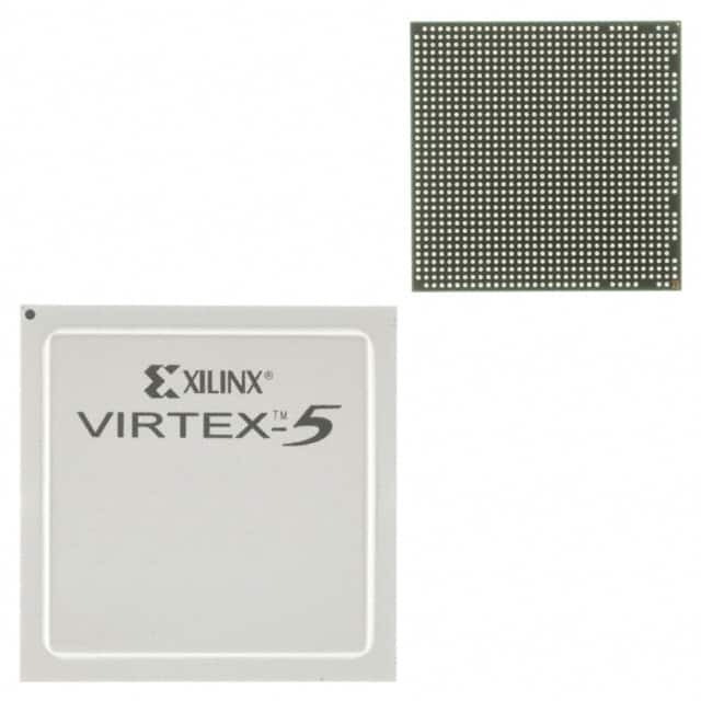
The XC5VLX30-3FF324C comes in a 324-pin Fine-Pitch Ball Grid Array (FBGA) package.
Essence
The essence of the XC5VLX30-3FF324C lies in its ability to provide a versatile and powerful platform for implementing complex digital designs.
Packaging/Quantity
The XC5VLX30-3FF324C is typically sold individually or in small quantities, depending on the supplier.
Specifications
- Logic Cells: 29,440
- Block RAM: 1,728 Kbits
- DSP Slices: 96
- Maximum Frequency: 550 MHz
- I/O Pins: 260
- Operating Voltage: 1.2V
Detailed Pin Configuration
The XC5VLX30-3FF324C has a total of 324 pins. These pins are used for various purposes, including input/output connections, power supply, configuration, and debugging. A detailed pin configuration diagram can be found in the product datasheet.
Functional Features
- High-speed data processing
- Configurable logic cells for custom designs
- On-chip memory blocks for efficient data storage
- Dedicated DSP slices for signal processing tasks
- Built-in clock management resources for precise timing control
Advantages and Disadvantages
Advantages
- Versatile and flexible design for a wide range of applications
- High-performance capabilities for demanding tasks
- Reconfigurable nature allows for easy updates and modifications
- Efficient use of resources with on-chip memory blocks and DSP slices
Disadvantages
- Higher cost compared to other programmable logic devices
- Steeper learning curve for beginners due to complexity
- Limited availability of alternative models with similar specifications
Working Principles
The XC5VLX30-3FF324C operates based on the principles of reconfigurable computing. It consists of an array of configurable logic cells that can be programmed to perform specific digital functions. These logic cells are interconnected through a network of programmable interconnects, allowing for the creation of complex digital designs. The FPGA can be programmed using Hardware Description Languages (HDL) such as VHDL or Verilog.
Detailed Application Field Plans
The XC5VLX30-3FF324C finds applications in various fields, including:
- Telecommunications: Used in high-speed data transmission systems and network infrastructure equipment.
- Aerospace and Defense: Employed in radar systems, avionics, and military communication systems.
- Industrial Automation: Utilized in control systems, robotics, and machine vision applications.
- Medical Devices: Integrated into medical imaging systems and diagnostic equipment.
- Research and Development: Used as a prototyping platform for developing custom digital designs.
Detailed and Complete Alternative Models
While the XC5VLX30-3FF324C offers unique features and specifications, there are alternative models available from other FPGA manufacturers. Some notable alternatives include:
- Altera Cyclone V E: Offers similar performance and flexibility.
- Lattice ECP5: Provides a low-power alternative with comparable capabilities.
- Microsemi SmartFusion2: Combines FPGA fabric with a microcontroller for added functionality.
These alternative models can be considered based on specific project requirements and cost considerations.
Word count: 533 words
Enumere 10 preguntas y respuestas comunes relacionadas con la aplicación de XC5VLX30-3FF324C en soluciones técnicas
Sure! Here are 10 common questions and answers related to the application of XC5VLX30-3FF324C in technical solutions:
Question: What is XC5VLX30-3FF324C?
- Answer: XC5VLX30-3FF324C is a specific model of Xilinx Virtex-5 FPGA (Field-Programmable Gate Array) with 30,000 logic cells.Question: What are the key features of XC5VLX30-3FF324C?
- Answer: Some key features include high-performance logic fabric, embedded PowerPC processors, DSP slices, and various I/O options.Question: What are the typical applications of XC5VLX30-3FF324C?
- Answer: XC5VLX30-3FF324C is commonly used in applications such as telecommunications, networking, industrial automation, and aerospace.Question: How can XC5VLX30-3FF324C be programmed?
- Answer: XC5VLX30-3FF324C can be programmed using Xilinx's Vivado Design Suite or ISE Design Suite software tools.Question: What is the power supply requirement for XC5VLX30-3FF324C?
- Answer: The recommended power supply voltage for XC5VLX30-3FF324C is typically 1.0V, but it can operate within a range of 0.95V to 1.05V.Question: Can XC5VLX30-3FF324C support multiple clock domains?
- Answer: Yes, XC5VLX30-3FF324C supports up to eight global clock networks, allowing for the implementation of multiple clock domains.Question: What is the maximum number of I/O pins available on XC5VLX30-3FF324C?
- Answer: XC5VLX30-3FF324C has a maximum of 324 I/O pins, which can be used for interfacing with external devices.Question: Does XC5VLX30-3FF324C have built-in memory resources?
- Answer: Yes, XC5VLX30-3FF324C has embedded Block RAM (BRAM) resources that can be used for storing data within the FPGA.Question: Can XC5VLX30-3FF324C be used in safety-critical applications?
- Answer: Yes, XC5VLX30-3FF324C can be used in safety-critical applications, but additional measures may be required to ensure functional safety.Question: Are there any known limitations or considerations when using XC5VLX30-3FF324C?
- Answer: Some considerations include power consumption, thermal management, and the need for proper signal integrity design practices to achieve optimal performance.
Please note that these answers are general and may vary depending on specific design requirements and implementation details.