

Consulte las especificaciones para obtener detalles del producto.
XC5VLX50T-1FFG665CES
Product Overview
Category
The XC5VLX50T-1FFG665CES belongs to the category of Field Programmable Gate Arrays (FPGAs).
Use
FPGAs are integrated circuits that can be programmed after manufacturing. They are widely used in various electronic applications, including telecommunications, automotive, aerospace, and consumer electronics.
Characteristics
The XC5VLX50T-1FFG665CES is known for its high performance and versatility. It offers a large number of configurable logic blocks, digital signal processing capabilities, and embedded memory resources. These features make it suitable for complex digital designs and signal processing tasks.
Package
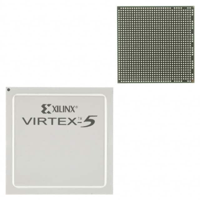
The XC5VLX50T-1FFG665CES comes in a compact package that ensures easy integration into electronic systems. The package type is Flip-Chip Fine-Pitch Ball Grid Array (FFG665).
Essence
The essence of the XC5VLX50T-1FFG665CES lies in its ability to provide reconfigurable hardware that can be customized for specific applications. This flexibility allows designers to implement complex functionality without the need for custom-designed ASICs.
Packaging/Quantity
The XC5VLX50T-1FFG665CES is typically packaged individually and is available in various quantities depending on the requirements of the customer or project.
Specifications
- Logic Cells: 49,920
- Block RAM: 2,592 Kbits
- DSP Slices: 240
- Maximum Frequency: 550 MHz
- I/O Pins: 665
- Operating Voltage: 1.0V
- Operating Temperature Range: -40°C to +100°C
Detailed Pin Configuration
The XC5VLX50T-1FFG665CES has a total of 665 I/O pins. These pins are used for input and output connections to other components in the system. The pin configuration is as follows:
- Pin 1: VCCINT
- Pin 2: GND
- Pin 3: IOL1PT0LN015
- Pin 4: IOL1NT0LN115
- ...
- Pin 665: IOL100NT2LN0VREF_15
Functional Features
The XC5VLX50T-1FFG665CES offers several functional features that enhance its performance and usability:
Configurable Logic Blocks (CLBs): These blocks provide the basic building blocks for implementing digital logic functions. The XC5VLX50T-1FFG665CES has a large number of CLBs, allowing for complex designs.
Digital Signal Processing (DSP) Slices: The DSP slices enable efficient implementation of mathematical operations commonly used in signal processing applications. They offer dedicated hardware resources for multiplication, addition, and accumulation.
Block RAM: The embedded memory resources in the XC5VLX50T-1FFG665CES allow for efficient storage and retrieval of data during operation. This feature is particularly useful in applications that require high-speed data processing.
High-Speed Interfaces: The FPGA supports various high-speed interfaces such as PCIe, Ethernet, and DDR3 memory interfaces, enabling seamless integration with other components in the system.
Advantages and Disadvantages
Advantages
- Flexibility: The reconfigurable nature of FPGAs allows for quick prototyping and design iterations.
- High Performance: The XC5VLX50T-1FFG665CES offers high-speed operation and can handle complex digital designs.
- Cost-Effective: FPGAs eliminate the need for custom ASICs, reducing development costs.
- Versatility: FPGAs can be used in a wide range of applications due to their programmability.
Disadvantages
- Power Consumption: FPGAs tend to consume more power compared to fixed-function ASICs.
- Complexity: Designing for FPGAs requires specialized knowledge and expertise.
- Limited Resources: The XC5VLX50T-1FFG665CES has a finite number of logic cells, which may restrict the complexity of designs that can be implemented.
Working Principles
FPGAs like the XC5VLX50T-1FFG665CES consist of an array of configurable logic blocks interconnected by programmable routing resources. These logic blocks can be programmed to implement various digital functions using a hardware description language (HDL) such as VHDL or Verilog. During operation, the FPGA is configured based on the desired functionality, allowing it to perform specific tasks.
Detailed Application Field Plans
The XC5VLX50T-1FFG665CES finds applications in various fields, including:
Telecommunications: FPGAs are used in base stations, routers, and network switches to handle high-speed data processing and protocol conversion tasks.
Automotive
Enumere 10 preguntas y respuestas comunes relacionadas con la aplicación de XC5VLX50T-1FFG665CES en soluciones técnicas
Sure! Here are 10 common questions and answers related to the application of XC5VLX50T-1FFG665CES in technical solutions:
Q1: What is XC5VLX50T-1FFG665CES? A1: XC5VLX50T-1FFG665CES is a field-programmable gate array (FPGA) manufactured by Xilinx. It is part of the Virtex-5 family and offers various features and capabilities for implementing complex digital designs.
Q2: What are the key specifications of XC5VLX50T-1FFG665CES? A2: The key specifications include 50,000 logic cells, 1,344 Kb of block RAM, 192 DSP slices, 400 MHz maximum clock frequency, and support for various I/O standards.
Q3: What are some typical applications of XC5VLX50T-1FFG665CES? A3: XC5VLX50T-1FFG665CES can be used in a wide range of applications such as high-performance computing, telecommunications, industrial automation, aerospace, and defense.
Q4: How can XC5VLX50T-1FFG665CES be programmed? A4: XC5VLX50T-1FFG665CES can be programmed using Xilinx's Vivado Design Suite or ISE Design Suite software tools. These tools allow designers to create and implement their digital designs on the FPGA.
Q5: What are the advantages of using XC5VLX50T-1FFG665CES in technical solutions? A5: Some advantages include high logic capacity, flexible I/O options, high-speed performance, low power consumption, and the ability to reconfigure the FPGA for different applications.
Q6: Can XC5VLX50T-1FFG665CES be used for real-time signal processing? A6: Yes, XC5VLX50T-1FFG665CES is capable of real-time signal processing due to its high-speed performance and dedicated digital signal processing (DSP) slices.
Q7: Is XC5VLX50T-1FFG665CES suitable for implementing complex algorithms? A7: Yes, XC5VLX50T-1FFG665CES is well-suited for implementing complex algorithms due to its large logic capacity, block RAM resources, and DSP slices.
Q8: Can XC5VLX50T-1FFG665CES interface with external devices? A8: Yes, XC5VLX50T-1FFG665CES supports various I/O standards and can interface with external devices such as sensors, memory modules, communication interfaces, and more.
Q9: What development boards or evaluation kits are available for XC5VLX50T-1FFG665CES? A9: Xilinx offers development boards and evaluation kits specifically designed for the Virtex-5 family, including XC5VLX50T-1FFG665CES. These kits provide a platform for prototyping and testing designs.
Q10: Are there any specific design considerations when using XC5VLX50T-1FFG665CES? A10: Some design considerations include power supply requirements, thermal management, clocking strategies, I/O voltage levels, and proper utilization of the FPGA's resources to optimize performance and functionality.
Please note that these questions and answers are general in nature and may vary depending on specific application requirements and design considerations.