

Consulte las especificaciones para obtener detalles del producto.
XC6SLX150-3FGG900C
Product Overview
Category
The XC6SLX150-3FGG900C belongs to the category of Field Programmable Gate Arrays (FPGAs).
Use
FPGAs are integrated circuits that can be programmed and reprogrammed to perform various digital functions. The XC6SLX150-3FGG900C is specifically designed for high-performance applications.
Characteristics
- High-performance FPGA with advanced features
- Large capacity and high-speed processing capabilities
- Flexible and reconfigurable design
- Low power consumption
- Suitable for complex digital designs
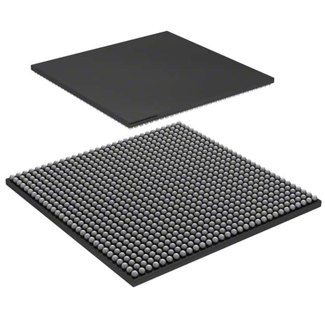
Package
The XC6SLX150-3FGG900C comes in a specific package known as the Fine-Pitch Ball Grid Array (FBGA). This package offers a compact form factor and excellent thermal performance.
Essence
The essence of the XC6SLX150-3FGG900C lies in its ability to provide a versatile and powerful platform for implementing complex digital designs.
Packaging/Quantity
The XC6SLX150-3FGG900C is typically sold in trays or reels, with each containing a specific quantity of FPGAs. The exact packaging and quantity may vary depending on the supplier.
Specifications
- FPGA Family: Spartan-6
- Logic Cells: 147,443
- Slice LUTs: 92,160
- Flip-Flops: 184,320
- Block RAM: 4,860 Kbits
- DSP Slices: 360
- Maximum Frequency: 550 MHz
- Operating Voltage: 1.2V
- I/O Standards: LVCMOS, LVTTL, HSTL, SSTL, LVDS, etc.
- Package Type: FBGA
- Package Pins: 900
- Temperature Range: -40°C to +100°C
Detailed Pin Configuration
The XC6SLX150-3FGG900C has a total of 900 pins, each serving a specific purpose in the FPGA's functionality. A detailed pin configuration diagram can be found in the product datasheet.
Functional Features
- High-speed serial connectivity
- Integrated memory blocks for efficient data storage
- Flexible clock management resources
- On-chip analog-to-digital converters (ADCs)
- Built-in digital signal processing (DSP) capabilities
- Support for various communication protocols (e.g., Ethernet, USB)
Advantages and Disadvantages
Advantages
- Versatile and reconfigurable design allows for flexibility in implementing complex digital systems.
- High-performance capabilities enable efficient processing of data-intensive applications.
- Low power consumption makes it suitable for power-sensitive designs.
- Extensive I/O standards support enables seamless integration with other components.
Disadvantages
- Steep learning curve for beginners due to the complexity of FPGA programming.
- Relatively higher cost compared to other programmable logic devices.
- Limited availability of alternative models with similar specifications.
Working Principles
The XC6SLX150-3FGG900C operates based on the principles of configurable logic and interconnects. The FPGA consists of an array of programmable logic cells interconnected through configurable routing resources. These logic cells can be programmed to implement desired digital functions by configuring the interconnections between them.
Detailed Application Field Plans
The XC6SLX150-3FGG900C finds applications in various fields, including: - Telecommunications: High-speed data processing and protocol conversion. - Aerospace and Defense: Radar and signal processing, image and video processing. - Industrial Automation: Control systems, motor control, and machine vision. - Medical Devices: Imaging and diagnostics equipment. - Research and Development: Prototyping and development of custom digital systems.
Detailed and Complete Alternative Models
While the XC6SLX150-3FGG900C offers a unique combination of features and specifications, there are alternative models available from other FPGA manufacturers. Some notable alternatives include: - Altera Cyclone series - Lattice Semiconductor ECP5 series - Microchip PolarFire series
These alternative models provide similar capabilities and can be considered based on specific project requirements.
Word count: 550 words
Enumere 10 preguntas y respuestas comunes relacionadas con la aplicación de XC6SLX150-3FGG900C en soluciones técnicas
Sure! Here are 10 common questions and answers related to the application of XC6SLX150-3FGG900C in technical solutions:
Question: What is XC6SLX150-3FGG900C?
- Answer: XC6SLX150-3FGG900C is a field-programmable gate array (FPGA) manufactured by Xilinx. It belongs to the Spartan-6 family and has 150,000 logic cells.Question: What are the key features of XC6SLX150-3FGG900C?
- Answer: Some key features include high-performance logic fabric, integrated memory blocks, DSP slices, clock management resources, and various I/O options.Question: What are the typical applications of XC6SLX150-3FGG900C?
- Answer: XC6SLX150-3FGG900C is commonly used in applications such as telecommunications, industrial automation, automotive electronics, medical devices, and aerospace systems.Question: How can XC6SLX150-3FGG900C be programmed?
- Answer: XC6SLX150-3FGG900C can be programmed using Xilinx's Vivado Design Suite or ISE Design Suite software tools. These tools allow users to design, simulate, and program the FPGA.Question: What is the power supply requirement for XC6SLX150-3FGG900C?
- Answer: The recommended power supply voltage for XC6SLX150-3FGG900C is 1.0V. However, it also supports a wide range of voltages from 0.95V to 1.15V.Question: Can XC6SLX150-3FGG900C interface with other components?
- Answer: Yes, XC6SLX150-3FGG900C has various I/O standards and interfaces such as LVCMOS, LVDS, PCI Express, DDR3, and more. It can easily interface with other components in a system.Question: What is the maximum operating frequency of XC6SLX150-3FGG900C?
- Answer: The maximum operating frequency of XC6SLX150-3FGG900C depends on the design and implementation. However, it can typically achieve frequencies up to several hundred megahertz (MHz) or even gigahertz (GHz).Question: Can XC6SLX150-3FGG900C be reprogrammed multiple times?
- Answer: Yes, XC6SLX150-3FGG900C is a reprogrammable FPGA, which means it can be programmed and reprogrammed multiple times to implement different designs or functionalities.Question: Are there any development boards available for XC6SLX150-3FGG900C?
- Answer: Yes, Xilinx provides development boards like the Spartan-6 FPGA SP601 Evaluation Kit, which can be used for prototyping and testing designs based on XC6SLX150-3FGG900C.Question: Where can I find more information about XC6SLX150-3FGG900C?
- Answer: You can find more detailed information about XC6SLX150-3FGG900C, including datasheets, user guides, and application notes, on Xilinx's official website or by contacting their technical support team.