

Consulte las especificaciones para obtener detalles del producto.
XC6SLX16-L1CPG196I
Basic Information Overview
- Category: Integrated Circuit (IC)
- Use: Programmable Logic Device (PLD)
- Characteristics:
- Low-power FPGA (Field-Programmable Gate Array)
- High-performance and high-capacity device
- Suitable for a wide range of applications
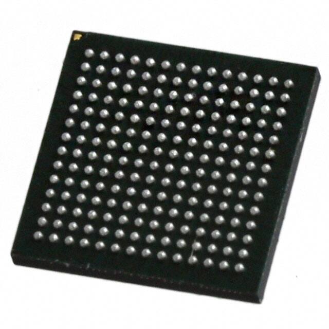
- Package: Ceramic Pin Grid Array (CPGA)
- Essence: The XC6SLX16-L1CPG196I is a versatile programmable logic device that offers high performance and low power consumption.
- Packaging/Quantity: The XC6SLX16-L1CPG196I is typically sold in trays or reels, with a quantity of 196 units per package.
Specifications
- Logic Cells: 14,579
- Slices: 2,160
- Flip-Flops: 34,560
- Block RAM: 576 Kb
- DSP48A1 Slices: 20
- I/O Pins: 154
- Operating Voltage: 1.2V
- Maximum Frequency: 400 MHz
- Configuration Memory: 4 Mb
- Package Type: 196-pin CPGA
Detailed Pin Configuration
The XC6SLX16-L1CPG196I has a total of 196 pins. These pins are used for various purposes, including input/output connections, clock signals, power supply, and configuration.
For the detailed pin configuration of XC6SLX16-L1CPG196I, please refer to the datasheet provided by the manufacturer.
Functional Features
- High-performance FPGA with low power consumption
- Flexible and reprogrammable logic cells
- Large number of I/O pins for interfacing with external devices
- On-chip memory blocks for efficient data storage
- Dedicated DSP slices for digital signal processing tasks
- Support for various communication protocols and interfaces
Advantages
- Versatile and suitable for a wide range of applications
- High-performance capabilities with low power consumption
- Ample logic cells, I/O pins, and memory blocks for complex designs
- Dedicated DSP slices for efficient digital signal processing
- Support for various communication protocols and interfaces
Disadvantages
- Relatively small compared to higher-end FPGAs in terms of logic capacity
- Limited number of DSP slices compared to specialized DSP chips
- Higher cost compared to simpler programmable logic devices
Working Principles
The XC6SLX16-L1CPG196I is based on the field-programmable gate array (FPGA) technology. It consists of an array of configurable logic cells that can be programmed to implement desired digital circuits. The device can be reprogrammed multiple times, allowing for flexibility in design.
The FPGA operates by configuring the interconnections between logic cells and implementing the desired functionality using look-up tables, flip-flops, and other components. The configuration data is stored in the on-chip configuration memory, which is loaded during startup.
Detailed Application Field Plans
The XC6SLX16-L1CPG196I finds applications in various fields, including: - Communications: Wireless base stations, network routers, and switches. - Industrial Control: Programmable logic controllers (PLCs), motor control systems, and automation equipment. - Aerospace and Defense: Avionics systems, radar signal processing, and secure communications. - Consumer Electronics: High-definition video processing, audio systems, and gaming consoles. - Medical Devices: Imaging systems, patient monitoring, and diagnostic equipment.
Detailed and Complete Alternative Models
- XC6SLX9-L1CPG196I
- XC6SLX25-L1CPG196I
- XC6SLX45-L1CPG196I
- XC6SLX75-L1CPG196I
- XC6SLX100-L1CPG196I
These alternative models offer different logic capacities, I/O pin counts, and performance levels to cater to specific design requirements.
Note: The content provided above is a sample structure for an encyclopedia entry. The actual content may vary based on the specific details and requirements of the XC6SLX16-L1CPG196I.
Enumere 10 preguntas y respuestas comunes relacionadas con la aplicación de XC6SLX16-L1CPG196I en soluciones técnicas
Sure! Here are 10 common questions and answers related to the application of XC6SLX16-L1CPG196I in technical solutions:
Q1: What is XC6SLX16-L1CPG196I? A1: XC6SLX16-L1CPG196I is a field-programmable gate array (FPGA) from Xilinx, which offers programmable logic and digital signal processing capabilities.
Q2: What are the key features of XC6SLX16-L1CPG196I? A2: Some key features of XC6SLX16-L1CPG196I include 16,640 logic cells, 576 Kb block RAM, 4 DSP slices, and support for various I/O standards.
Q3: What are the typical applications of XC6SLX16-L1CPG196I? A3: XC6SLX16-L1CPG196I is commonly used in applications such as industrial automation, telecommunications, automotive electronics, medical devices, and aerospace systems.
Q4: How can XC6SLX16-L1CPG196I be programmed? A4: XC6SLX16-L1CPG196I can be programmed using Xilinx's Vivado Design Suite or ISE Design Suite software tools.
Q5: What are the power requirements for XC6SLX16-L1CPG196I? A5: XC6SLX16-L1CPG196I typically operates at a voltage range of 1.14V to 1.26V, with a maximum power consumption of around 2.5W.
Q6: Can XC6SLX16-L1CPG196I interface with other components or devices? A6: Yes, XC6SLX16-L1CPG196I supports various communication protocols such as SPI, I2C, UART, and Ethernet, allowing it to interface with other components or devices.
Q7: What is the maximum clock frequency supported by XC6SLX16-L1CPG196I? A7: The maximum clock frequency supported by XC6SLX16-L1CPG196I is typically around 450 MHz, depending on the design and implementation.
Q8: Can XC6SLX16-L1CPG196I be used for real-time signal processing? A8: Yes, XC6SLX16-L1CPG196I's DSP slices and high-speed I/O capabilities make it suitable for real-time signal processing applications.
Q9: Does XC6SLX16-L1CPG196I have any built-in security features? A9: Yes, XC6SLX16-L1CPG196I offers built-in AES encryption and tamper detection features to enhance system security.
Q10: Are there any development boards available for XC6SLX16-L1CPG196I? A10: Yes, Xilinx provides development boards like the Spartan-6 FPGA SP601 Evaluation Kit, which can be used for prototyping and testing with XC6SLX16-L1CPG196I.
Please note that the specific details and answers may vary based on the context and requirements of the technical solution.