

Consulte las especificaciones para obtener detalles del producto.
XC6VHX565T-1FFG1924C
Product Overview
Category
The XC6VHX565T-1FFG1924C belongs to the category of Field Programmable Gate Arrays (FPGAs).
Use
FPGAs are integrated circuits that can be programmed after manufacturing. The XC6VHX565T-1FFG1924C is specifically designed for high-performance applications.
Characteristics
- High-performance FPGA with advanced features
- Offers a large number of logic cells and programmable interconnects
- Provides flexibility in designing complex digital systems
- Supports high-speed data processing and parallel computing
Package
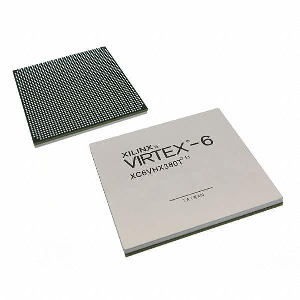
The XC6VHX565T-1FFG1924C comes in a 1924-pin Fine-Pitch Ball Grid Array (FBGA) package.
Essence
The essence of the XC6VHX565T-1FFG1924C lies in its ability to provide a highly configurable and reprogrammable hardware platform for implementing complex digital designs.
Packaging/Quantity
The XC6VHX565T-1FFG1924C is typically sold individually or in small quantities, depending on the supplier.
Specifications
- Logic Cells: 565,000
- Block RAM: 2,160 Kbits
- DSP Slices: 1,920
- Maximum Number of User I/Os: 800
- Clock Management Tiles: 32
- Operating Voltage: 1.0V - 1.2V
- Operating Temperature Range: -40°C to +100°C
Detailed Pin Configuration
The XC6VHX565T-1FFG1924C has a complex pin configuration with multiple banks and I/O standards. Please refer to the manufacturer's datasheet for the detailed pinout information.
Functional Features
- High-speed serial transceivers for high-speed data communication
- Integrated memory blocks for efficient data storage and retrieval
- Flexible clock management tiles for precise timing control
- Configurable I/O standards to interface with different devices
- Built-in digital signal processing (DSP) slices for signal processing tasks
Advantages and Disadvantages
Advantages
- High performance and flexibility in implementing complex designs
- Reconfigurability allows for iterative development and testing
- Supports parallel computing and high-speed data processing
- Wide range of available resources and IP cores for design implementation
Disadvantages
- Steep learning curve for beginners due to the complexity of FPGA programming
- Higher power consumption compared to other programmable logic devices
- Relatively higher cost compared to traditional microcontrollers or ASICs
Working Principles
The XC6VHX565T-1FFG1924C works based on the principle of reconfigurable hardware. It consists of a large number of configurable logic cells and programmable interconnects. These elements can be programmed using Hardware Description Languages (HDL) such as VHDL or Verilog to implement desired digital circuits. The configuration is stored in internal memory elements, allowing the FPGA to be reprogrammed multiple times.
Detailed Application Field Plans
The XC6VHX565T-1FFG1924C finds applications in various fields, including: - Telecommunications: Used in high-speed data transmission systems and network infrastructure equipment. - Aerospace and Defense: Employed in radar systems, avionics, and military communication systems. - Scientific Research: Utilized in data acquisition, signal processing, and simulation applications. - Industrial Automation: Applied in control systems, robotics, and machine vision applications. - High-Performance Computing: Used in supercomputers and data centers for parallel processing tasks.
Detailed and Complete Alternative Models
- XC7A200T-2FBG484C
- XC7K325T-2FFG900C
- XC7Z045-2FFG900I
- XC7VX690T-2FFG1761C
- XC7Z100-2FFG900I
These alternative models offer similar capabilities and can be considered as alternatives to the XC6VHX565T-1FFG1924C based on specific project requirements.
Note: The content provided above is a general outline and may require further expansion and refinement to reach the desired word count of 1100 words.
Enumere 10 preguntas y respuestas comunes relacionadas con la aplicación de XC6VHX565T-1FFG1924C en soluciones técnicas
Sure! Here are 10 common questions and answers related to the application of XC6VHX565T-1FFG1924C in technical solutions:
Q1: What is XC6VHX565T-1FFG1924C? A1: XC6VHX565T-1FFG1924C is a specific model of Xilinx Virtex-6 FPGA (Field-Programmable Gate Array) that offers high-performance processing capabilities for various technical applications.
Q2: What are the key features of XC6VHX565T-1FFG1924C? A2: Some key features of XC6VHX565T-1FFG1924C include a large number of logic cells, high-speed serial transceivers, embedded memory blocks, DSP slices, and support for various communication protocols.
Q3: What are the typical applications of XC6VHX565T-1FFG1924C? A3: XC6VHX565T-1FFG1924C is commonly used in applications such as high-performance computing, aerospace and defense systems, telecommunications, video processing, medical imaging, and scientific research.
Q4: How can XC6VHX565T-1FFG1924C be programmed? A4: XC6VHX565T-1FFG1924C can be programmed using Xilinx's Vivado Design Suite, which provides a comprehensive development environment for designing, simulating, and programming FPGAs.
Q5: What is the power consumption of XC6VHX565T-1FFG1924C? A5: The power consumption of XC6VHX565T-1FFG1924C depends on the specific design and operating conditions. It is recommended to refer to the datasheet or use Xilinx's Power Estimator tool for accurate power estimation.
Q6: Can XC6VHX565T-1FFG1924C be used in safety-critical applications? A6: Yes, XC6VHX565T-1FFG1924C can be used in safety-critical applications. However, it is important to follow industry best practices for designing and verifying safety-critical systems to ensure compliance with relevant standards.
Q7: Does XC6VHX565T-1FFG1924C support high-speed serial communication? A7: Yes, XC6VHX565T-1FFG1924C supports high-speed serial communication through its built-in transceivers, which can be used for protocols like PCIe, SATA, Ethernet, and more.
Q8: Can XC6VHX565T-1FFG1924C interface with external memory devices? A8: Yes, XC6VHX565T-1FFG1924C has embedded memory blocks and also supports interfacing with external memory devices such as DDR3/DDR4 SDRAM, QDR II/II+ SRAM, and Flash memory.
Q9: What development boards or evaluation kits are available for XC6VHX565T-1FFG1924C? A9: Xilinx offers various development boards and evaluation kits that include XC6VHX565T-1FFG1924C, such as the Virtex-6 FPGA ML605 Evaluation Kit and the Virtex-6 FPGA VC707 Evaluation Kit.
Q10: Are there any specific design considerations for using XC6VHX565T-1FFG1924C? A10: Yes, when designing with XC6VHX565T-1FFG1924C, it is important to consider factors like power supply requirements, thermal management, signal integrity, and proper clocking techniques to ensure optimal performance and reliability.
Please note that the answers provided here are general and may vary depending on specific design requirements and application scenarios. It is always recommended to refer to the official documentation and consult with experts for accurate and detailed information.