

Consulte las especificaciones para obtener detalles del producto.
XC6VLX195T-L1FFG1156C
Product Overview
Category
The XC6VLX195T-L1FFG1156C belongs to the category of Field-Programmable Gate Arrays (FPGAs).
Use
FPGAs are integrated circuits that can be programmed and reprogrammed to perform various digital functions. The XC6VLX195T-L1FFG1156C is specifically designed for high-performance applications that require complex logic and processing capabilities.
Characteristics
- High-performance FPGA with advanced features
- Large capacity and high-speed processing capabilities
- Flexible and reconfigurable design
- Suitable for demanding applications in industries such as telecommunications, aerospace, and defense
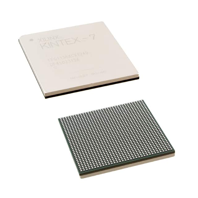
Package
The XC6VLX195T-L1FFG1156C comes in a compact package that ensures easy integration into electronic systems. It is designed to be mounted on a printed circuit board (PCB) and connected to other components.
Essence
The essence of the XC6VLX195T-L1FFG1156C lies in its ability to provide a customizable and powerful digital processing platform. Its programmable nature allows designers to implement complex algorithms and functions tailored to their specific requirements.
Packaging/Quantity
The XC6VLX195T-L1FFG1156C is typically packaged individually and is available in various quantities depending on the manufacturer or distributor.
Specifications
- Logic Cells: 195,000
- Flip-Flops: 486,000
- Block RAM: 4,860 Kb
- DSP Slices: 740
- Maximum Frequency: 550 MHz
- I/O Pins: 1,156
- Operating Voltage: 1.0V - 1.2V
- Package Type: FF1156
Detailed Pin Configuration
The XC6VLX195T-L1FFG1156C has a comprehensive pin configuration that enables connectivity with other components. The pins are organized into different banks, each serving specific functions such as input, output, or power supply.
For a detailed pin configuration diagram and description, please refer to the product datasheet provided by the manufacturer.
Functional Features
The XC6VLX195T-L1FFG1156C offers several functional features that make it suitable for a wide range of applications:
- High-speed processing: With a maximum frequency of 550 MHz, the FPGA can handle complex computations and data processing tasks efficiently.
- Reconfigurability: The FPGA's programmable nature allows designers to modify and update the functionality of the device without the need for hardware changes.
- Versatile I/O capabilities: The XC6VLX195T-L1FFG1156C provides a large number of I/O pins, enabling seamless integration with external devices and systems.
- Advanced DSP capabilities: The FPGA includes dedicated digital signal processing (DSP) slices, allowing for efficient implementation of algorithms commonly used in signal processing applications.
Advantages and Disadvantages
Advantages
- High-performance processing capabilities
- Flexibility and reconfigurability
- Large capacity for complex designs
- Suitable for demanding applications
Disadvantages
- Steeper learning curve compared to traditional fixed-function integrated circuits
- Higher cost compared to off-the-shelf microcontrollers or processors
- Requires specialized design tools and expertise for programming and development
Working Principles
The XC6VLX195T-L1FFG1156C operates based on the principles of digital logic. It consists of an array of configurable logic blocks (CLBs), interconnected by programmable routing resources. These CLBs can be programmed to implement various logical functions, arithmetic operations, and memory elements.
Designers use Hardware Description Languages (HDLs) such as VHDL or Verilog to describe the desired functionality of the FPGA. The HDL code is then synthesized and mapped onto the XC6VLX195T-L1FFG1156C, resulting in a configuration bitstream that defines the behavior of the FPGA.
During operation, the FPGA executes the programmed logic, performing the desired functions based on the input signals and internal state.
Detailed Application Field Plans
The XC6VLX195T-L1FFG1156C finds applications in various industries and domains, including:
- Telecommunications: Used in high-speed data processing, network routing, and protocol handling.
- Aerospace: Employed in satellite communication systems, radar signal processing, and avionics.
- Defense: Utilized for secure communications, encryption/decryption, and radar systems.
- Industrial Automation: Applied in control systems, robotics, and machine vision.
- Medical Imaging: Used for real-time image processing and analysis in medical devices.
These are just a few examples, and the versatility of the XC6VLX195T-L1FFG1156C allows it to be adapted to many other application fields.
Alternative
Enumere 10 preguntas y respuestas comunes relacionadas con la aplicación de XC6VLX195T-L1FFG1156C en soluciones técnicas
Sure! Here are 10 common questions and answers related to the application of XC6VLX195T-L1FFG1156C in technical solutions:
Q1: What is XC6VLX195T-L1FFG1156C? A1: XC6VLX195T-L1FFG1156C is a field-programmable gate array (FPGA) from Xilinx. It is a high-performance device with 195,000 logic cells and various features suitable for complex technical solutions.
Q2: What are the key features of XC6VLX195T-L1FFG1156C? A2: Some key features include high logic capacity, advanced DSP capabilities, multiple I/O standards, integrated memory controllers, and support for various communication protocols.
Q3: What are the typical applications of XC6VLX195T-L1FFG1156C? A3: XC6VLX195T-L1FFG1156C is commonly used in applications such as telecommunications, aerospace, defense, industrial automation, medical imaging, and high-performance computing.
Q4: How can XC6VLX195T-L1FFG1156C be programmed? A4: XC6VLX195T-L1FFG1156C can be programmed using Xilinx's Vivado Design Suite or ISE Design Suite. These software tools provide a graphical interface and HDL-based design flow for programming the FPGA.
Q5: What is the power consumption of XC6VLX195T-L1FFG1156C? A5: The power consumption of XC6VLX195T-L1FFG1156C depends on the specific configuration and usage. It is recommended to refer to the datasheet and power estimation tools provided by Xilinx for accurate power consumption information.
Q6: Can XC6VLX195T-L1FFG1156C be used in safety-critical applications? A6: Yes, XC6VLX195T-L1FFG1156C can be used in safety-critical applications. However, it is important to follow appropriate design practices and consider additional measures for functional safety, such as redundancy and fault tolerance.
Q7: Does XC6VLX195T-L1FFG1156C support high-speed serial communication? A7: Yes, XC6VLX195T-L1FFG1156C supports high-speed serial communication through its integrated transceivers. It provides support for protocols like PCIe, SATA, Ethernet, and more.
Q8: Can XC6VLX195T-L1FFG1156C interface with external memory devices? A8: Yes, XC6VLX195T-L1FFG1156C has integrated memory controllers that allow it to interface with various external memory devices, including DDR3, DDR2, and QDR II+.
Q9: What development boards or evaluation kits are available for XC6VLX195T-L1FFG1156C? A9: Xilinx offers development boards and evaluation kits specifically designed for XC6VLX195T-L1FFG1156C, such as the ML605 and KC705 boards. These provide a platform for prototyping and testing designs.
Q10: Are there any known limitations or considerations when using XC6VLX195T-L1FFG1156C? A10: It is recommended to carefully review the datasheet and user guides provided by Xilinx for specific limitations and considerations related to XC6VLX195T-L1FFG1156C. Some common considerations include power management, thermal dissipation, and signal integrity.