

Consulte las especificaciones para obtener detalles del producto.
XC6VLX365T-1FF1759I
Product Overview
Category
The XC6VLX365T-1FF1759I belongs to the category of Field-Programmable Gate Arrays (FPGAs).
Use
FPGAs are integrated circuits that can be programmed after manufacturing. They are widely used in various electronic applications, including telecommunications, automotive, aerospace, and consumer electronics.
Characteristics
The XC6VLX365T-1FF1759I is known for its high performance and versatility. It offers a large number of programmable logic cells, on-chip memory, and various I/O interfaces. These features make it suitable for complex digital designs and signal processing tasks.
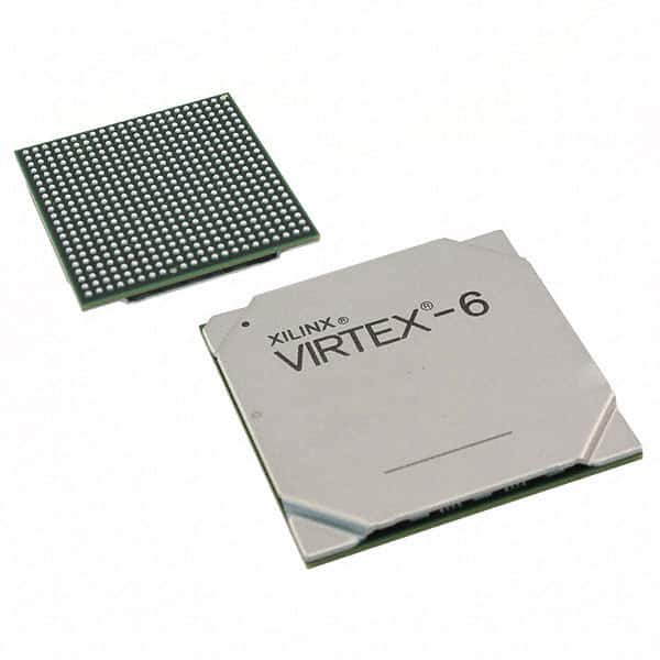
Package
The XC6VLX365T-1FF1759I is available in a compact package, which ensures easy integration into electronic systems. The package provides protection against environmental factors and facilitates efficient heat dissipation.
Essence
The essence of the XC6VLX365T-1FF1759I lies in its ability to provide flexible and customizable digital circuitry. Its programmability allows designers to implement complex algorithms and functions without the need for custom-designed ASICs.
Packaging/Quantity
The XC6VLX365T-1FF1759I is typically sold in trays or reels, depending on the manufacturer's packaging standards. The quantity per package may vary, but it is commonly available in quantities suitable for both prototyping and production purposes.
Specifications
- FPGA Family: Virtex-6
- Logic Cells: 365,000
- Block RAM: 13,200 Kb
- DSP Slices: 740
- Maximum I/O Count: 800
- Operating Voltage: 1.0V
- Operating Temperature Range: -40°C to 100°C
- Package Type: Flip-Chip FineLine BGA
- Package Pins: 1759
Detailed Pin Configuration
The XC6VLX365T-1FF1759I has a comprehensive pin configuration, allowing for versatile connectivity. The detailed pinout information can be found in the manufacturer's datasheet or reference manual.
Functional Features
High Performance
The XC6VLX365T-1FF1759I offers high-speed performance, enabling rapid data processing and efficient execution of complex algorithms. It is capable of handling demanding applications that require real-time processing and low latency.
Flexible I/O Interfaces
With a maximum I/O count of 800, the XC6VLX365T-1FF1759I provides a wide range of interfaces, including LVCMOS, LVTTL, LVDS, and differential signaling. This flexibility allows seamless integration with various external devices and systems.
On-Chip Memory
The FPGA includes a substantial amount of on-chip memory, providing efficient storage for intermediate results, lookup tables, and configuration data. This feature eliminates the need for external memory components, reducing system complexity and cost.
DSP Slices
The XC6VLX365T-1FF1759I incorporates dedicated Digital Signal Processing (DSP) slices, which are optimized for arithmetic operations commonly used in signal processing applications. These slices enhance the FPGA's capability to perform complex mathematical calculations efficiently.
Advantages and Disadvantages
Advantages
- High-performance FPGA suitable for demanding applications.
- Versatile I/O interfaces enable seamless integration with various systems.
- On-chip memory reduces the need for external memory components.
- Dedicated DSP slices enhance signal processing capabilities.
Disadvantages
- Relatively higher power consumption compared to lower-end FPGAs.
- Steeper learning curve for designers unfamiliar with FPGA programming.
Working Principles
The XC6VLX365T-1FF1759I operates based on the principles of reconfigurable logic. It consists of a matrix of programmable logic cells and interconnects that can be configured to implement desired digital circuits. The configuration is stored in on-chip memory and can be modified as needed.
During operation, the FPGA reads input signals, processes them using the programmed logic, and generates output signals accordingly. The flexibility of FPGAs allows for rapid prototyping, iterative design improvements, and customization without the need for hardware redesign.
Detailed Application Field Plans
The XC6VLX365T-1FF1759I finds applications in various fields, including:
Telecommunications
- Baseband processing in wireless communication systems.
- Network packet processing and routing.
- Protocol conversion and adaptation.
Automotive
- Advanced driver-assistance systems (ADAS).
- In-vehicle infotainment (IVI) systems.
- Engine control units (ECUs).
Aerospace
- Avionics systems.
- Radar signal processing.
- Satellite communication systems.
Consumer Electronics
- High-definition video processing.
- Gaming consoles.
- Audio and video streaming devices.
Detailed and Complete Alternative Models
- Xilinx Virt
Enumere 10 preguntas y respuestas comunes relacionadas con la aplicación de XC6VLX365T-1FF1759I en soluciones técnicas
Sure! Here are 10 common questions and answers related to the application of XC6VLX365T-1FF1759I in technical solutions:
Q1: What is XC6VLX365T-1FF1759I? A1: XC6VLX365T-1FF1759I is a specific model of Field Programmable Gate Array (FPGA) manufactured by Xilinx.
Q2: What are the key features of XC6VLX365T-1FF1759I? A2: Some key features of XC6VLX365T-1FF1759I include high logic capacity, advanced DSP capabilities, multiple I/O standards, and low power consumption.
Q3: What are the typical applications of XC6VLX365T-1FF1759I? A3: XC6VLX365T-1FF1759I is commonly used in various technical solutions such as telecommunications, networking, industrial automation, aerospace, and defense.
Q4: How does XC6VLX365T-1FF1759I benefit technical solutions? A4: XC6VLX365T-1FF1759I offers high performance, flexibility, and reconfigurability, allowing for efficient implementation of complex algorithms and designs.
Q5: What programming languages can be used with XC6VLX365T-1FF1759I? A5: XC6VLX365T-1FF1759I can be programmed using hardware description languages (HDLs) such as VHDL or Verilog.
Q6: Can XC6VLX365T-1FF1759I be used for real-time signal processing? A6: Yes, XC6VLX365T-1FF1759I's advanced DSP capabilities make it suitable for real-time signal processing applications.
Q7: What is the power consumption of XC6VLX365T-1FF1759I? A7: The power consumption of XC6VLX365T-1FF1759I depends on the specific design and configuration, but it is generally known for its low power consumption.
Q8: Can XC6VLX365T-1FF1759I be used in high-reliability applications? A8: Yes, XC6VLX365T-1FF1759I is designed to meet the requirements of high-reliability applications, making it suitable for use in critical systems.
Q9: Are there any development tools available for XC6VLX365T-1FF1759I? A9: Yes, Xilinx provides a range of development tools, such as Vivado Design Suite, that support the design and programming of XC6VLX365T-1FF1759I.
Q10: Can XC6VLX365T-1FF1759I be used in combination with other FPGAs or integrated circuits? A10: Yes, XC6VLX365T-1FF1759I can be used in combination with other FPGAs or integrated circuits to create more complex and scalable solutions.
Please note that these answers are general and may vary depending on specific application requirements.