

Consulte las especificaciones para obtener detalles del producto.
XC7A200T-1FB484I
Product Overview
Category
The XC7A200T-1FB484I belongs to the category of Field Programmable Gate Arrays (FPGAs).
Use
FPGAs are integrated circuits that can be programmed and reprogrammed to perform various digital functions. The XC7A200T-1FB484I is specifically designed for high-performance applications that require complex logic functions.
Characteristics
- High-performance FPGA with advanced programmability
- Large capacity and high-speed processing capabilities
- Flexible and customizable design options
- Low power consumption
- Suitable for a wide range of applications
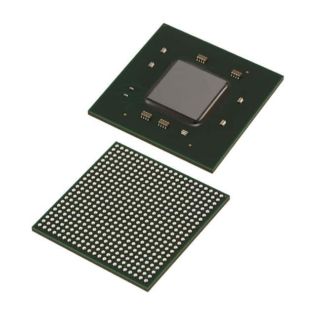
Package
The XC7A200T-1FB484I comes in a FB484 package, which refers to the type of chip packaging used. This package provides a compact and robust enclosure for the FPGA.
Essence
The essence of the XC7A200T-1FB484I lies in its ability to provide a versatile and powerful platform for implementing complex digital designs. It offers a high level of customization and performance, making it suitable for demanding applications.
Packaging/Quantity
The XC7A200T-1FB484I is typically sold individually or in small quantities, depending on the supplier. It is packaged in anti-static bags or trays to ensure proper handling and protection during transportation.
Specifications
- FPGA Family: Xilinx 7 Series
- Device Type: Artix-7
- Logic Cells: 215,360
- Look-Up Tables (LUTs): 135,000
- Flip-Flops: 270,000
- Block RAM: 4,860 Kbits
- DSP Slices: 740
- Maximum Operating Frequency: 800 MHz
- I/O Pins: 400
- Voltage Range: 0.95V - 1.05V
Detailed Pin Configuration
The XC7A200T-1FB484I has a total of 400 I/O pins, each serving a specific purpose in the FPGA's functionality. The pin configuration is detailed in the device datasheet provided by the manufacturer.
Functional Features
1. High Performance
The XC7A200T-1FB484I offers exceptional performance with its large number of logic cells, look-up tables, and flip-flops. This enables the implementation of complex digital designs and ensures efficient processing of data.
2. Flexibility and Customization
With its programmable nature, the XC7A200T-1FB484I allows users to customize their designs according to specific requirements. This flexibility makes it suitable for a wide range of applications, from telecommunications to industrial automation.
3. Low Power Consumption
The XC7A200T-1FB484I is designed to minimize power consumption while maintaining high performance. This feature is particularly beneficial for battery-powered devices or applications where energy efficiency is crucial.
Advantages and Disadvantages
Advantages
- High-performance capabilities
- Flexible and customizable design options
- Low power consumption
- Suitable for a wide range of applications
Disadvantages
- Relatively higher cost compared to other programmable logic devices
- Steeper learning curve for programming and utilizing the full potential of the FPGA
Working Principles
The XC7A200T-1FB484I operates based on the principles of reconfigurable computing. It consists of an array of configurable logic blocks interconnected through programmable routing resources. These resources can be programmed to create desired digital circuits, allowing for the implementation of complex functions.
Detailed Application Field Plans
The XC7A200T-1FB484I finds applications in various fields, including:
- Telecommunications: Used in base stations, routers, and network switches to handle high-speed data processing and routing.
- Industrial Automation: Employed in control systems, robotics, and machine vision applications for real-time data processing and control.
- Aerospace and Defense: Utilized in radar systems, avionics, and military communication equipment for their high-performance computing capabilities.
- Medical Imaging: Used in medical devices such as ultrasound machines and MRI scanners to process and analyze imaging data.
Detailed and Complete Alternative Models
- XC7A100T-1FGG484C
- XC7A35T-1CPG236C
- XC7A50T-1CSG324I
- XC7A75T-1FGG484I
- XC7A15T-1FTG256C
These alternative models offer varying capacities and features to cater to different application requirements. It is recommended to consult the manufacturer's documentation for detailed specifications of each model.
Word count: 610 words
Enumere 10 preguntas y respuestas comunes relacionadas con la aplicación de XC7A200T-1FB484I en soluciones técnicas
Sure! Here are 10 common questions and answers related to the application of XC7A200T-1FB484I in technical solutions:
1. What is XC7A200T-1FB484I? - XC7A200T-1FB484I is a field-programmable gate array (FPGA) from Xilinx, specifically from the Artix-7 family. It offers a high-performance, low-power solution for various applications.
2. What are the key features of XC7A200T-1FB484I? - Some key features of XC7A200T-1FB484I include a large number of programmable logic cells, high-speed I/O interfaces, embedded memory blocks, DSP slices, and support for various communication protocols.
3. What are the typical applications of XC7A200T-1FB484I? - XC7A200T-1FB484I can be used in a wide range of applications such as industrial automation, aerospace and defense systems, medical devices, telecommunications, video processing, and high-performance computing.
4. What is the maximum operating frequency of XC7A200T-1FB484I? - The maximum operating frequency of XC7A200T-1FB484I depends on the specific design and implementation. However, it can typically achieve frequencies in the range of several hundred megahertz to a few gigahertz.
5. How much logic capacity does XC7A200T-1FB484I offer? - XC7A200T-1FB484I has a logic capacity of approximately 215,360 logic cells, which can be used to implement complex digital designs.
6. Can XC7A200T-1FB484I interface with external devices? - Yes, XC7A200T-1FB484I supports various high-speed I/O interfaces such as PCIe, Ethernet, USB, and DDR3 memory interfaces, allowing it to interface with external devices.
7. What development tools are available for programming XC7A200T-1FB484I? - Xilinx provides Vivado Design Suite, which is a comprehensive development environment for designing, implementing, and programming FPGAs like XC7A200T-1FB484I.
8. Can XC7A200T-1FB484I be reprogrammed after deployment? - Yes, XC7A200T-1FB484I is a field-programmable device, meaning it can be reprogrammed even after it has been deployed in a system.
9. Does XC7A200T-1FB484I support partial reconfiguration? - Yes, XC7A200T-1FB484I supports partial reconfiguration, allowing specific portions of the FPGA to be reprogrammed while the rest of the design remains operational.
10. What power supply requirements does XC7A200T-1FB484I have? - XC7A200T-1FB484I typically requires a single 1.0V core voltage supply and a separate 2.5V or 3.3V auxiliary voltage supply for I/O interfaces.
Please note that the answers provided here are general and may vary depending on the specific implementation and requirements of your technical solution.