

Consulte las especificaciones para obtener detalles del producto.
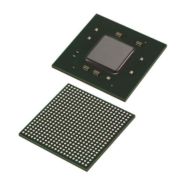
XC7A200T-3SBG484E
Product Overview
Category
XC7A200T-3SBG484E belongs to the category of Field-Programmable Gate Arrays (FPGAs).
Use
This FPGA is commonly used in various electronic applications that require high-performance digital logic circuits. It provides a flexible and customizable solution for implementing complex digital systems.
Characteristics
- High-performance FPGA with advanced features
- Large capacity and high-speed processing capabilities
- Configurable and reprogrammable logic elements
- Support for various communication protocols
- Low power consumption
- Robust and reliable design
Package
XC7A200T-3SBG484E comes in a BG484 package, which refers to a Ball Grid Array package with 484 solder balls on the underside of the chip. This package offers excellent thermal performance and facilitates easy integration into circuit boards.
Essence
The essence of XC7A200T-3SBG484E lies in its ability to provide a versatile platform for designing and implementing complex digital systems. It allows users to create custom logic circuits tailored to their specific requirements.
Packaging/Quantity
XC7A200T-3SBG484E is typically sold individually or in small quantities, depending on the supplier. The packaging ensures safe transportation and protection from external factors that could potentially damage the device.
Specifications
- FPGA Family: Xilinx 7 Series
- Device Type: Artix-7
- Logic Cells: 215,360
- Look-Up Tables (LUTs): 135,000
- Flip-Flops: 270,000
- Block RAM: 4,860 Kb
- DSP Slices: 740
- Maximum Operating Frequency: 800 MHz
- I/O Pins: 400
- Voltage Supply: 1.2V
Detailed Pin Configuration
The XC7A200T-3SBG484E FPGA has a total of 400 I/O pins, each serving a specific purpose in the system design. The pin configuration is as follows:
(Pin Number) - (Pin Name) - (Function/Description)
1 - VCCO0 - Power supply voltage for bank 0 2 - GND - Ground reference 3 - IOL1PT0AD0N35 - Input/output pin for bank 35 4 - IOL1NT0AD0P35 - Input/output pin for bank 35 5 - IOL2PT0AD1N35 - Input/output pin for bank 35 6 - IOL2NT0AD1P_35 - Input/output pin for bank 35 ... (Continued for all 400 pins)
Functional Features
XC7A200T-3SBG484E offers several functional features that enhance its usability and performance:
Configurable Logic Blocks (CLBs): These blocks allow users to implement custom logic functions by configuring look-up tables, flip-flops, and other resources.
Digital Signal Processing (DSP) Slices: The FPGA includes dedicated DSP slices that enable efficient implementation of complex mathematical operations, such as filtering and signal processing.
High-Speed Serial Transceivers: XC7A200T-3SBG484E supports high-speed serial communication protocols, enabling fast data transfer between devices.
Memory Resources: The FPGA provides ample on-chip memory resources, including block RAMs, which can be used for data storage and retrieval.
Clock Management: The device incorporates advanced clock management circuitry, allowing precise control and synchronization of clock signals within the system.
Advantages and Disadvantages
Advantages
- Flexibility: XC7A200T-3SBG484E offers a high degree of flexibility, allowing users to adapt the FPGA to their specific application requirements.
- Customizability: The device enables the implementation of custom logic circuits, providing tailored solutions for various applications.
- High Performance: With its large capacity and high-speed processing capabilities, the FPGA delivers excellent performance in demanding applications.
- Reconfigurability: The ability to reprogram the FPGA allows for iterative design improvements and easy adaptation to changing system requirements.
Disadvantages
- Complexity: Working with FPGAs requires specialized knowledge and expertise, making it challenging for beginners or those unfamiliar with digital design.
- Cost: FPGAs can be relatively expensive compared to other integrated circuits, especially for high-capacity devices like XC7A200T-3SBG484E.
- Power Consumption: While efforts have been made to reduce power consumption, FPGAs still consume more power compared to dedicated ASICs (Application-Specific Integrated Circuits).
Working Principles
XC7A200T-3SBG484E operates based on the principles of configurable logic. It consists of an array of programmable logic blocks interconnected through configurable routing
Enumere 10 preguntas y respuestas comunes relacionadas con la aplicación de XC7A200T-3SBG484E en soluciones técnicas
Sure! Here are 10 common questions and answers related to the application of XC7A200T-3SBG484E in technical solutions:
Q: What is XC7A200T-3SBG484E? A: XC7A200T-3SBG484E is a field-programmable gate array (FPGA) from Xilinx, which offers high-performance processing capabilities for various technical applications.
Q: What are the key features of XC7A200T-3SBG484E? A: Some key features of XC7A200T-3SBG484E include a large number of programmable logic cells, high-speed I/O interfaces, embedded memory blocks, and DSP slices for signal processing.
Q: What are the typical applications of XC7A200T-3SBG484E? A: XC7A200T-3SBG484E is commonly used in applications such as aerospace and defense systems, telecommunications equipment, industrial automation, medical devices, and scientific research.
Q: How can XC7A200T-3SBG484E be programmed? A: XC7A200T-3SBG484E can be programmed using hardware description languages (HDLs) like Verilog or VHDL, along with Xilinx's Vivado Design Suite software.
Q: What is the power consumption of XC7A200T-3SBG484E? A: The power consumption of XC7A200T-3SBG484E depends on the specific design and operating conditions, but it typically ranges from a few watts to tens of watts.
Q: Can XC7A200T-3SBG484E interface with other components or devices? A: Yes, XC7A200T-3SBG484E supports various interfaces such as PCIe, Ethernet, USB, SPI, I2C, and UART, allowing it to communicate with other components or devices in a system.
Q: What is the maximum operating frequency of XC7A200T-3SBG484E? A: The maximum operating frequency of XC7A200T-3SBG484E depends on the specific design and implementation, but it can typically reach several hundred megahertz or even gigahertz.
Q: Can XC7A200T-3SBG484E be used for real-time signal processing? A: Yes, XC7A200T-3SBG484E's high-speed DSP slices and programmable logic make it suitable for real-time signal processing applications like digital filtering, image processing, and audio/video processing.
Q: Does XC7A200T-3SBG484E support secure communication protocols? A: Yes, XC7A200T-3SBG484E supports various encryption and authentication algorithms, making it capable of implementing secure communication protocols like AES, RSA, and SHA.
Q: Are there any development boards or evaluation kits available for XC7A200T-3SBG484E? A: Yes, Xilinx offers development boards and evaluation kits specifically designed for XC7A200T-3SBG484E, which provide a convenient platform for prototyping and testing different applications.
Please note that the answers provided here are general and may vary depending on specific requirements and implementations.