

Consulte las especificaciones para obtener detalles del producto.
XC7K325T-1FBG900I
Product Overview
Category
XC7K325T-1FBG900I belongs to the category of Field Programmable Gate Arrays (FPGAs).
Use
FPGAs are integrated circuits that can be programmed and reprogrammed to perform various digital functions. They are widely used in industries such as telecommunications, automotive, aerospace, and consumer electronics.
Characteristics
XC7K325T-1FBG900I is a high-performance FPGA with advanced features and capabilities. It offers a large number of programmable logic cells, high-speed I/O interfaces, and embedded memory blocks. This FPGA is designed to handle complex digital designs and provide flexibility for customization.
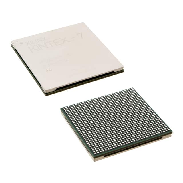
Package
XC7K325T-1FBG900I comes in a BGA (Ball Grid Array) package. The BGA package provides better thermal performance and improved electrical characteristics compared to other packaging options.
Essence
The essence of XC7K325T-1FBG900I lies in its ability to provide a highly configurable and flexible platform for implementing digital designs. It allows designers to create custom logic circuits and optimize their performance according to specific requirements.
Packaging/Quantity
XC7K325T-1FBG900I is typically sold in trays or reels, depending on the manufacturer's packaging standards. The quantity per package may vary, but it is commonly available in quantities suitable for both prototyping and production purposes.
Specifications
- FPGA Family: Kintex-7
- Device: XC7K325T
- Logic Cells: 325,000
- DSP Slices: 1,920
- Block RAM: 36 Mb
- Maximum I/O Count: 500
- Operating Voltage: 0.95V - 1.05V
- Operating Temperature: -40°C to 100°C
- Package Type: FBG900I
Detailed Pin Configuration
The detailed pin configuration of XC7K325T-1FBG900I can be found in the manufacturer's datasheet. It provides information about the specific functions and connections of each pin on the FPGA.
Functional Features
XC7K325T-1FBG900I offers several functional features that make it a versatile FPGA for various applications:
- High-performance programmable logic cells for complex digital designs.
- Flexible I/O interfaces supporting various standards such as LVCMOS, LVDS, and differential signaling.
- Embedded memory blocks for efficient data storage and retrieval.
- Dedicated DSP slices for implementing high-speed signal processing algorithms.
- Clock management resources for precise timing control.
- Configurable power management options for optimizing power consumption.
Advantages and Disadvantages
Advantages
- High-performance and flexibility for implementing complex digital designs.
- Large number of logic cells and memory blocks for customization.
- Support for various I/O standards and high-speed interfaces.
- Efficient power management options for optimizing power consumption.
- Reliable BGA packaging for improved thermal performance.
Disadvantages
- Higher cost compared to other programmable logic devices.
- Steeper learning curve for beginners due to its advanced features.
- Limited availability of alternative models with similar specifications.
Working Principles
XC7K325T-1FBG900I operates based on the principles of reconfigurable computing. It consists of an array of programmable logic cells interconnected through configurable routing resources. The functionality of the FPGA is determined by the configuration bitstream loaded into it, which defines the interconnections and behavior of the logic cells.
During operation, the FPGA executes the programmed logic circuits by routing signals through the interconnect fabric and performing computations using the logic cells. The input and output signals are processed according to the defined logic functions, allowing the FPGA to perform a wide range of digital tasks.
Detailed Application Field Plans
XC7K325T-1FBG900I finds applications in various fields, including:
- Telecommunications: Used in base stations, routers, and network switches for high-speed data processing and protocol handling.
- Automotive: Employed in advanced driver assistance systems (ADAS) for real-time image processing and sensor fusion.
- Aerospace: Utilized in satellite communication systems, radar signal processing, and avionics for reliable and efficient data processing.
- Consumer Electronics: Integrated into high-performance gaming consoles, video processing devices, and multimedia systems for enhanced functionality and performance.
Detailed and Complete Alternative Models
While XC7K325T-1FBG900I is a highly capable FPGA, there are alternative models available with similar specifications. Some notable alternatives include:
- Xilinx Virtex-7 series FPGAs
- Intel Stratix 10 series FPGAs
- Lattice ECP5 series FPGAs
- Microsemi SmartFusion2 series FPGAs
These alternative models offer comparable features and performance, providing designers with options
Enumere 10 preguntas y respuestas comunes relacionadas con la aplicación de XC7K325T-1FBG900I en soluciones técnicas
Sure! Here are 10 common questions and answers related to the application of XC7K325T-1FBG900I in technical solutions:
Q1: What is XC7K325T-1FBG900I? A1: XC7K325T-1FBG900I is a specific model of Xilinx's Kintex-7 FPGA (Field-Programmable Gate Array) family. It offers a high-performance, low-power solution for various applications.
Q2: What are the key features of XC7K325T-1FBG900I? A2: Some key features include a large number of programmable logic cells, high-speed serial transceivers, integrated memory blocks, DSP slices, and support for various communication protocols.
Q3: What are the typical applications of XC7K325T-1FBG900I? A3: XC7K325T-1FBG900I can be used in a wide range of applications such as wireless communication systems, video processing, industrial automation, medical imaging, aerospace, and defense.
Q4: How does XC7K325T-1FBG900I benefit wireless communication systems? A4: XC7K325T-1FBG900I provides high-speed serial transceivers that enable efficient data transmission, while its programmable logic allows for flexible implementation of wireless protocols and algorithms.
Q5: Can XC7K325T-1FBG900I handle video processing tasks? A5: Yes, XC7K325T-1FBG900I has sufficient resources to handle video processing tasks such as image enhancement, compression, and real-time video analytics.
Q6: What advantages does XC7K325T-1FBG900I offer in industrial automation? A6: XC7K325T-1FBG900I's high-performance capabilities and support for various communication protocols make it suitable for implementing advanced control systems, monitoring devices, and industrial networking.
Q7: How does XC7K325T-1FBG900I contribute to medical imaging applications? A7: XC7K325T-1FBG900I can be used to accelerate image processing algorithms, enabling real-time analysis of medical images and improving the overall efficiency of medical imaging systems.
Q8: Can XC7K325T-1FBG900I be used in aerospace and defense applications? A8: Yes, XC7K325T-1FBG900I is well-suited for aerospace and defense applications due to its high reliability, low power consumption, and ability to handle complex signal processing tasks.
Q9: What are the programming options for XC7K325T-1FBG900I? A9: XC7K325T-1FBG900I can be programmed using Xilinx's Vivado Design Suite, which provides a comprehensive set of tools for FPGA design, synthesis, simulation, and implementation.
Q10: Are there any specific design considerations when using XC7K325T-1FBG900I? A10: Yes, designers should consider factors such as power supply requirements, thermal management, I/O compatibility, and system integration when incorporating XC7K325T-1FBG900I into their technical solutions.
Please note that these questions and answers are general in nature and may vary depending on specific application requirements.