

Consulte las especificaciones para obtener detalles del producto.
XC7S50-2FTGB196I
Product Overview
Category
The XC7S50-2FTGB196I belongs to the category of Field Programmable Gate Arrays (FPGAs).
Use
FPGAs are integrated circuits that can be programmed and reprogrammed to perform various digital functions. The XC7S50-2FTGB196I is specifically designed for high-performance applications that require complex logic functions.
Characteristics
- High-performance FPGA with advanced features
- Flexible and reprogrammable design
- Supports complex logic functions
- Offers high-speed data processing capabilities
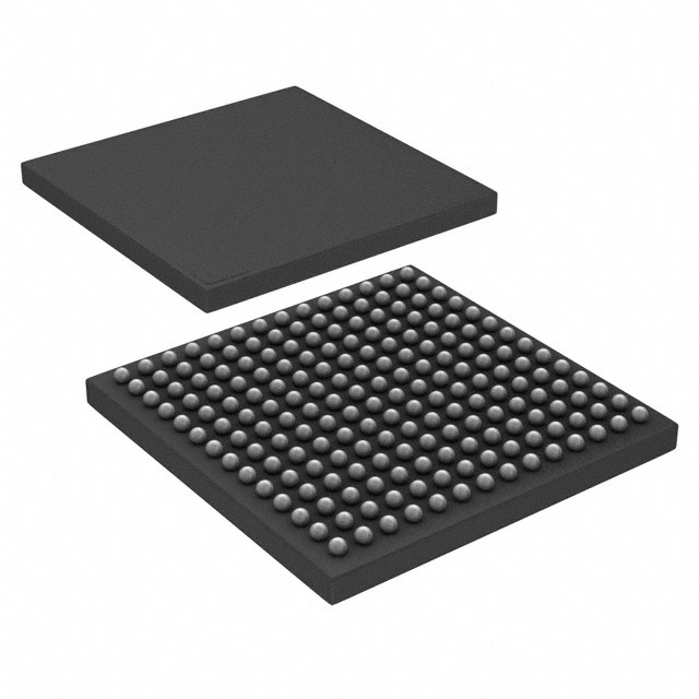
Package
The XC7S50-2FTGB196I comes in a compact package that ensures easy integration into electronic systems. It is designed to be mounted on a printed circuit board (PCB) using surface mount technology (SMT).
Essence
The essence of the XC7S50-2FTGB196I lies in its ability to provide a customizable and versatile solution for implementing complex digital logic functions in various applications.
Packaging/Quantity
The XC7S50-2FTGB196I is typically packaged in reels or trays, depending on the manufacturer's specifications. The quantity per package may vary, but it is commonly available in quantities suitable for both prototyping and production purposes.
Specifications
- FPGA Family: Xilinx 7 Series
- Device Type: Spartan-7
- Logic Cells: 52,160
- Flip-Flops: 32,768
- Block RAM: 1,800 Kbits
- DSP Slices: 80
- I/O Pins: 196
- Operating Voltage: 1.2V
- Speed Grade: -2
- Temperature Range: Industrial (-40°C to +100°C)
Detailed Pin Configuration
The XC7S50-2FTGB196I has a total of 196 I/O pins, each serving a specific purpose in the system. The pin configuration is detailed in the device datasheet provided by the manufacturer.
Functional Features
- High-performance FPGA with advanced logic capabilities
- Configurable I/O standards for interfacing with various devices
- Built-in memory blocks for efficient data storage and retrieval
- Dedicated digital signal processing (DSP) slices for complex mathematical operations
- Flexible clock management resources for precise timing control
- Support for various communication protocols, such as PCIe, Ethernet, and USB
Advantages and Disadvantages
Advantages
- Versatile and reprogrammable design allows for flexibility in implementing different functions.
- High-performance capabilities enable complex logic operations and data processing.
- Extensive I/O options facilitate easy integration with other components and systems.
- Availability of development tools and support from the manufacturer's ecosystem.
Disadvantages
- Relatively higher power consumption compared to simpler logic devices.
- Steeper learning curve for beginners due to the complexity of FPGA programming.
- Higher cost compared to traditional fixed-function integrated circuits.
Working Principles
The XC7S50-2FTGB196I operates based on the principles of field-programmable gate arrays. It consists of an array of configurable logic blocks (CLBs), interconnected by programmable routing resources. The CLBs can be programmed to implement desired logic functions, while the routing resources allow for interconnection between different blocks.
The FPGA is programmed using a hardware description language (HDL), such as VHDL or Verilog. The HDL code describes the desired functionality, which is then synthesized and implemented onto the FPGA using specialized software tools. Once programmed, the FPGA can perform the specified logic functions.
Detailed Application Field Plans
The XC7S50-2FTGB196I finds applications in various fields that require high-performance digital logic capabilities. Some of the detailed application field plans include:
Communications: The FPGA can be used in networking equipment, such as routers and switches, to handle high-speed data processing and protocol conversion tasks.
Industrial Automation: It can be employed in industrial control systems for real-time monitoring, process control, and automation tasks.
Aerospace and Defense: The FPGA's reprogrammable nature makes it suitable for applications in radar systems, avionics, and military communication systems.
Medical Devices: It can be utilized in medical imaging equipment, patient monitoring systems, and laboratory instruments that require high-speed data processing and complex algorithms.
Automotive: The FPGA can be integrated into automotive electronics for functions like advanced driver assistance systems (ADAS), infotainment systems, and engine control units (ECUs).
Detailed and Complete Alternative Models
- XC7S15-1FTGB196I
- XC7S25-1FTGB196I
- XC7S35-1FTGB196I
- XC7S100-1FTGB196I
- XC7S200-1FTGB196I
These alternative models offer varying levels of
Enumere 10 preguntas y respuestas comunes relacionadas con la aplicación de XC7S50-2FTGB196I en soluciones técnicas
Sure! Here are 10 common questions and answers related to the application of XC7S50-2FTGB196I in technical solutions:
Q: What is XC7S50-2FTGB196I? A: XC7S50-2FTGB196I is a specific model of Xilinx Spartan-7 FPGA (Field-Programmable Gate Array) with 50,000 logic cells.
Q: What are the key features of XC7S50-2FTGB196I? A: Some key features include 50,000 logic cells, 2.5V core voltage, 196-pin Fine-Pitch Ball Grid Array (FBGA) package, and various I/O interfaces.
Q: What are the typical applications of XC7S50-2FTGB196I? A: XC7S50-2FTGB196I can be used in a wide range of applications such as industrial automation, automotive electronics, telecommunications, medical devices, and more.
Q: How can XC7S50-2FTGB196I be programmed? A: XC7S50-2FTGB196I can be programmed using Xilinx's Vivado Design Suite or other compatible programming tools.
Q: What is the maximum operating frequency of XC7S50-2FTGB196I? A: The maximum operating frequency of XC7S50-2FTGB196I depends on the specific design and implementation, but it can typically reach several hundred megahertz.
Q: Can XC7S50-2FTGB196I interface with external devices? A: Yes, XC7S50-2FTGB196I supports various I/O standards and can interface with external devices such as sensors, displays, memory modules, and communication interfaces.
Q: What are the power requirements for XC7S50-2FTGB196I? A: XC7S50-2FTGB196I requires a 2.5V core voltage and typically consumes around 1-2 watts of power, depending on the design and operating conditions.
Q: Can XC7S50-2FTGB196I be used in safety-critical applications? A: Yes, XC7S50-2FTGB196I can be used in safety-critical applications as long as proper design techniques and safety measures are implemented.
Q: Are there any development boards available for XC7S50-2FTGB196I? A: Yes, Xilinx offers development boards specifically designed for Spartan-7 FPGAs, including models that support XC7S50-2FTGB196I.
Q: Where can I find more information about XC7S50-2FTGB196I? A: You can find more detailed information about XC7S50-2FTGB196I in the official documentation provided by Xilinx, including datasheets, user guides, and application notes.